ChipApex | Global Electronic Components Supplier

SEARCH
Search Product
Search Post
— IC芯片 | 连接器 | 传感器 | 被动器件 —
Search productSearch post
— IC芯片 | 连接器 | 传感器 | 被动器件 —
Consult the customer manager about the wholesale price.
consultation hotline:86-132-6715-2157
email:[email protected]
Contact the product manager for consultation. One-stop consultation is available.
Do you want a lower wholesale price? Please send us your inquiry and we will reply immediately.
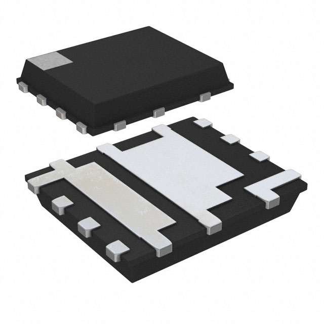
The NTMFD4C86NT3G is a PowerPhase dual N-channel MOSFET in a DFN8 (5x6 mm) package. It integrates a high-side FET (Q1) and a low-side FET (Q2). Q1 offers a maximum drain current of 20 A with an on-resistance of 5.4 mΩ at VGS=10V. Q2 supports up to 32 A with an on-resistance of 2.6 mΩ at VGS=10V. Both devices feature a 30 V drain-to-source breakdown voltage. The co-packaged design minimizes parasitic inductances and board space, optimizing power loss for efficient switching applications.
Verify the specific ordering suffix against official documentation to confirm packaging details. The NTMFD4C86NT3G variant corresponds to a tape and reel quantity of 5000 units in the DFN8 package. Confirming the exact suffix ensures alignment with required shipping specifications and handling procedures.
Select this component for designs requiring a compact dual-N-channel configuration with distinct high-side and low-side current capabilities. The integrated layout reduces external component count and loop inductance. Ensure gate drive voltages align with the specified thresholds for optimal RDS(on) performance across the operating temperature range.
This part belongs to the PowerPhase series from onsemi, which focuses on integrating complementary MOSFETs into single packages. This approach simplifies PCB layout and improves thermal management compared to discrete solutions. The DFN8 footprint provides a balance between thermal dissipation and spatial efficiency for modern power electronics.
Direct substitutes include the NTMFD4C86NT1G, which shares identical electrical characteristics but differs in packaging quantity (1500 units per tape and reel). Verify pinout compatibility and thermal resistance values when transitioning between these variants.
The high-side FET (Q1) has a continuous drain current rating of 20 A, while the low-side FET (Q2) supports 32 A under steady-state conditions at 25°C.
The DFN8 package minimizes parasitic inductances due to its co-packaged design, which enhances switching speed and reduces electromagnetic interference in high-frequency applications.
Both the high-side and low-side FETs share a maximum drain-to-source voltage (V(BR)DSS) rating of 30 V.
 NTMFD4C86NT3G

The activity of extra discounts on wholesale prices is in full swing…
Please fill in your contact information and we will send you the latest wholesale price list.