 ChipApex | Global Electronic Components Supplier

SEARCH
Search Product
Search Post
— IC芯片 | 连接器 | 传感器 | 被动器件 —
Search productSearch post
— IC芯片 | 连接器 | 传感器 | 被动器件 —
Consult the customer manager about the wholesale price.
consultation hotline:86-132-6715-2157
email:[email protected]
Contact the product manager for consultation. One-stop consultation is available.
Do you want a lower wholesale price? Please send us your inquiry and we will reply immediately.
The NTQD6866R2 is an N-Channel Power MOSFET array manufactured by onsemi, housed in a TSSOP-8 surface-mount package. It features dual independent channels with a maximum drain-source voltage (Vds) of 20 Volts and a continuous drain current (Id) of 4.7 Amperes per channel. The device has a maximum gate-source threshold voltage (Vgs(th)) of 1.2 Volts at 250µA and a maximum gate charge (Qg) of 22nC at 4.5V. Input capacitance (Ciss) is rated at 1400pF maximum at 16V. The component supports a junction temperature range from -55°C to 150°C and offers a maximum power dissipation of 940mW.
Verify the specific ordering suffix matches the required tape and reel quantity, typically 4000 units per reel as documented in official distribution channels. Confirm that the component meets RoHS standards and check for any automotive or industrial qualification markings if required by the target application environment. Ensure the supplier provides valid traceability documentation consistent with onsemi manufacturing records.
Select this component when a dual-channel solution is needed for low-voltage, high-current applications. The 20V rating suits systems operating below this threshold, while the 4.7A current capability handles moderate load requirements. Consider the TSSOP-8 footprint for PCB layout constraints and evaluate the thermal management needs given the 940mW power dissipation limit in the specified package.
This part belongs to the onsemi Power MOSFET portfolio, specifically designed as a dual-array device. It complements other low-voltage transistors in the manufacturer's lineup, offering integrated dual-channel functionality to reduce component count compared to using discrete single-channel MOSFETs in similar voltage and current ranges.
Consult official onsemi cross-reference documents for verified substitutes. No public substitute part numbers are confirmed in the provided source material.
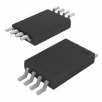 NTQD6866R2

The activity of extra discounts on wholesale prices is in full swing…
Please fill in your contact information and we will send you the latest wholesale price list.





