ChipApex | Global Electronic Components Supplier

SEARCH
Search Product
Search Post
— IC芯片 | 连接器 | 传感器 | 被动器件 —
Search productSearch post
— IC芯片 | 连接器 | 传感器 | 被动器件 —
Consult the customer manager about the wholesale price.
consultation hotline:86-132-6715-2157
email:[email protected]
Contact the product manager for consultation. One-stop consultation is available.
Do you want a lower wholesale price? Please send us your inquiry and we will reply immediately.
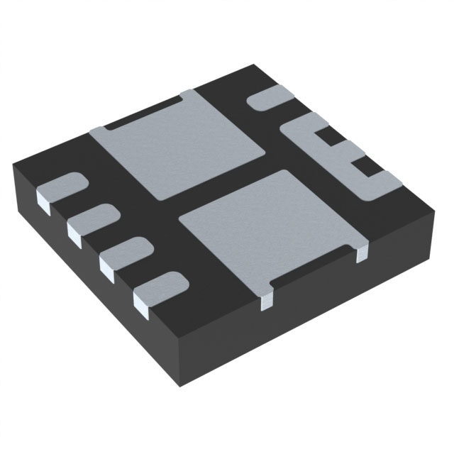
The NTTFD2D8N03P1E is a symmetric dual N-channel Power MOSFET from onsemi, utilizing PowerTrench and Power Clip technologies. It features a compact WQFN12 (3.3mm x 3.3mm) package. Key electrical parameters include a drain-to-source voltage of 30V and a maximum continuous drain current of 80A at TC = 25°C. The device offers low on-resistance, with RDS(on) max values of 2.5mΩ at VGS = 10V and 3.0mΩ at VGS = 4.5V. Total gate charge is typically 9.5nC at VGS = 4.5V and 20.8nC at VGS = 10V. It operates within a junction temperature range of -55°C to +150°C.
Verify the specific ordering suffix against the manufacturer's official documentation to ensure correct packaging specifications. Confirm that the component meets all relevant environmental compliance standards required by the target market. Review the datasheet for accurate tape and reel dimensions before integrating into automated assembly lines.
Evaluate the thermal resistance characteristics relative to the intended PCB copper pad size and layout. Ensure the gate drive voltage aligns with the specified thresholds for optimal RDS(on) performance. Consider the pulsed drain current capabilities when designing for transient load conditions or avalanche energy scenarios.
This component belongs to onsemi's PowerTrench family of N-channel MOSFETs. It is designed for high-efficiency power switching applications where low conduction losses and fast switching speeds are critical. The symmetric dual structure allows for efficient half-bridge or synchronous rectifier configurations.
Direct substitutes must match the 30V rating, dual N-channel configuration, and WQFN12 package dimensions. Verify equivalent RDS(on) and QG values to maintain circuit efficiency. Check pinout compatibility to ensure seamless integration without PCB redesign.
The maximum continuous drain current is 80A for both Q1 and Q2 at TC = 25°C.
Yes, the device is 100% UIS tested. Q1 can handle 55.4 mJ and Q2 can handle 58.8 mJ of single pulse avalanche energy.
The typical total gate charge is 9.5nC for Q1 and 9.3nC for Q2 under standard test conditions.
 NTTFD2D8N03P1E

The activity of extra discounts on wholesale prices is in full swing…
Please fill in your contact information and we will send you the latest wholesale price list.