ChipApex | Global Electronic Components Supplier

SEARCH
Search Product
Search Post
— IC芯片 | 连接器 | 传感器 | 被动器件 —
Search productSearch post
— IC芯片 | 连接器 | 传感器 | 被动器件 —
Consult the customer manager about the wholesale price.
consultation hotline:86-132-6715-2157
email:[email protected]
Contact the product manager for consultation. One-stop consultation is available.
Do you want a lower wholesale price? Please send us your inquiry and we will reply immediately.
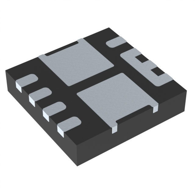
The onsemi NTTFD4D0N04HLTWG is a dual N-channel MOSFET device integrating two specialized transistors within a single package. It features an internal connection to the switching node, facilitating placement and routing for synchronous buck converters. The control MOSFET (Q2) and synchronous MOSFET (Q1) are optimized for power efficiency. Key electrical parameters include a maximum drain-source voltage of 40V for both devices. At VGS=10V and ID=10A, the maximum RDS(on) is 4.5mΩ; at VGS=4.5V and ID=8.0A, it is 7mΩ. Continuous drain current is 60A at TC=25°C and 37A at TC=100°C.
Verify the specific suffix 'TWG' against official documentation to confirm tape-and-reel packaging details. Ensure compatibility with RoHS standards as indicated for the base part number. Cross-reference pinout definitions for the DFN-5L package to prevent installation errors during assembly.
Select this component for designs requiring compact integration of high-side and low-side switches in synchronous rectification topologies. Evaluate thermal performance based on the specified continuous current ratings at case temperatures. Consider the low on-resistance characteristics for minimizing conduction losses in power conversion circuits.
This device belongs to onsemi's portfolio of discrete semiconductors, specifically within the MOSFET category. It is designed for power management applications where space-saving dual configurations are beneficial. The product line supports various industrial and consumer electronics requiring efficient DC-DC conversion.
Publicly confirmed substitute part numbers for NTTFD4D0N04HLTWG are not available in the provided data. Verify functional equivalence with other dual N-channel MOSFETs from onsemi or other manufacturers if direct substitution is required.
 NTTFD4D0N04HLTWG

The activity of extra discounts on wholesale prices is in full swing…
Please fill in your contact information and we will send you the latest wholesale price list.