 ChipApex | Global Electronic Components Supplier

SEARCH
Search Product
Search Post
— IC芯片 | 连接器 | 传感器 | 被动器件 —
Search productSearch post
— IC芯片 | 连接器 | 传感器 | 被动器件 —
Consult the customer manager about the wholesale price.
consultation hotline:86-132-6715-2157
email:[email protected]
Contact the product manager for consultation. One-stop consultation is available.
Do you want a lower wholesale price? Please send us your inquiry and we will reply immediately.
The NTZD3155CT2G is a dual N/P-channel enhancement mode MOSFET manufactured by onsemi. It features a maximum drain-source voltage of 20 V and continuous drain currents of 450 mA for the N-channel and 570 mA for the P-channel. The device utilizes an SOT-563 surface-mount package with six pins. Key electrical parameters include a maximum on-resistance of 2 Ω for the N-channel and 900 mΩ for the P-channel, with a typical gate charge of 0.1 nC at 4.5 V for the N-channel and 1.5 nC at 4.5 V for the P-channel. It operates within a temperature range of -55 °C to +150 °C.
Verify the specific suffix 'T2G' against official manufacturer documentation to confirm tape-and-reel packaging specifications. Ensure compatibility with standard SOT-563 footprint dimensions during PCB layout. Confirm RoHS compliance status through current datasheets as manufacturing processes may evolve over time.
Select this component when space-constrained designs require both N-type and P-type switching functions. Evaluate thermal performance based on the 280 mW power dissipation limit. Compare on-resistance values against system efficiency requirements to ensure adequate current handling for the intended load conditions.
This part belongs to onsemi's portfolio of small-signal MOSFETs designed for general-purpose switching. It serves as a complementary pair solution, reducing component count compared to using discrete single transistors. The SOT-563 package allows for automated assembly in high-volume manufacturing environments.
Publicly confirmed substitute part numbers for NTZD3155CT2G were not identified in the provided reference data. Verify pinout compatibility and electrical ratings before considering alternative manufacturers or series.
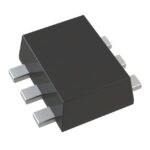 NTZD3155CT2G

The activity of extra discounts on wholesale prices is in full swing…
Please fill in your contact information and we will send you the latest wholesale price list.





