 ChipApex | Global Electronic Components Supplier

SEARCH
Search Product
Search Post
— IC芯片 | 连接器 | 传感器 | 被动器件 —
Search productSearch post
— IC芯片 | 连接器 | 传感器 | 被动器件 —
Consult the customer manager about the wholesale price.
consultation hotline:86-132-6715-2157
email:[email protected]
Contact the product manager for consultation. One-stop consultation is available.
Do you want a lower wholesale price? Please send us your inquiry and we will reply immediately.
The NVMD4N03R2G is a dual N-channel power MOSFET manufactured by onsemi, housed in an SO-8 surface-mount package. It features a drain-to-source voltage (VDSS) of 30 V and a continuous drain current (ID) of 4.0 A at 25 °C. The device exhibits ultra-low on-resistance, with typical values of 0.048 Ω at VGS = 10 V and 0.065 Ω at VGS = 4.5 V. It supports a single-pulse avalanche energy (EAS) of 80 mJ and operates within a junction temperature range of -55 °C to +150 °C. The component is Pb-Free, RoHS compliant, and qualified under AEC-Q101 standards.
Verify the specific ordering suffix 'R2G' corresponds to the required tape and reel packaging quantity of 2500 units per manufacturer specifications. Confirm that the NVMD prefix aligns with project requirements for automotive qualification and unique site control changes. Ensure compatibility with standard SOIC-8 soldering profiles and thermal management constraints defined in the datasheet maximum ratings.
Select this component for designs requiring dual N-channel isolation within a compact footprint. Evaluate the 0.048 Ω on-resistance at 10 V gate drive against system efficiency targets. Consider the 30 V breakdown voltage margin relative to supply rails. Verify thermal dissipation capabilities using the specified junction-to-ambient resistance for the intended PCB pad size and ambient conditions.
This part belongs to the NTMD4N03/NVMD4N03 family of dual N-channel power MOSFETs. The NVMD prefix specifically denotes devices intended for automotive and other applications requiring unique site and control change requirements, distinguishing it from the standard NTMD variant which lacks these specific qualification markers.
NTMD4N03R2G serves as the non-automotive equivalent within the same electrical specification family. Both parts share identical pinouts and performance metrics but differ in manufacturing site controls and automotive qualification status.
The typical static drain-to-source on-state resistance (RDS(on)) is 0.065 Ω when measured at VGS = 4.5 Vdc and ID = 2 Adc.
Style 11 defines the pinout: Pin 1 is Source 1, Pin 2 is Gate 1, Pin 3 is Source 2, Pin 4 is Gate 2, Pins 5 and 6 are Drain 2, and Pins 7 and 8 are Drain 1.
Yes, the diode is explicitly characterized for use in bridge circuits and exhibits high-speed operation with soft recovery characteristics to minimize noise and switching losses.
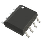 NVMD4N03R2G

The activity of extra discounts on wholesale prices is in full swing…
Please fill in your contact information and we will send you the latest wholesale price list.





