ChipApex | Global Electronic Components Supplier

SEARCH
Search Product
Search Post
— IC芯片 | 连接器 | 传感器 | 被动器件 —
Search productSearch post
— IC芯片 | 连接器 | 传感器 | 被动器件 —
Consult the customer manager about the wholesale price.
consultation hotline:86-132-6715-2157
email:[email protected]
Contact the product manager for consultation. One-stop consultation is available.
Do you want a lower wholesale price? Please send us your inquiry and we will reply immediately.
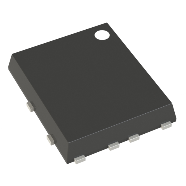
The onsemi NVMFD5C674NLT1G is a dual N-channel enhancement mode power MOSFET housed in an 8-pin PowerTDFN package measuring 5x6 mm. It features a drain-source voltage rating of 60 V and a continuous drain current of 42 A at case temperature of 25 °C, reducing to 26 A at 100 °C. The device exhibits a maximum on-resistance of 20.4 mΩ at VGS = 4.5 V and 11.7 mΩ typical at VGS = 10 V. Maximum gate-source voltage is ±20 V, with a threshold voltage range of 1.2 V to 2.2 V. Thermal performance includes a junction-to-case thermal resistance of 2.86 °C/W and a maximum power dissipation of 37 W at 25 °C case temperature.
Verify the specific suffix against official datasheets to confirm package variations or tape-and-reel specifications. Confirm RoHS compliance status and lead times directly with authorized distributors. Ensure storage conditions meet manufacturer recommendations to prevent moisture sensitivity issues prior to soldering.
Select this component when space constraints require a small surface-mount package alongside high current handling capabilities. Evaluate thermal management requirements based on the specified junction-to-case resistance. Compare gate charge values against driver capabilities to ensure efficient switching speeds without excessive drive current demands.
This part belongs to the NVMFD5C6xxNL series of dual MOSFETs from onsemi. The series shares common packaging dimensions and automotive qualification standards. Variations within the series typically involve differences in on-resistance and current ratings while maintaining the same physical envelope and pinout configuration.
Direct substitutes include other 60V dual N-channel MOSFETs in 5x6mm DFN packages with comparable RDS(on) and ID ratings. Verify pin compatibility and thermal characteristics before substitution. Check for equivalent AEC-Q101 certification if automotive applications are involved.
 NVMFD5C674NLT1G

The activity of extra discounts on wholesale prices is in full swing…
Please fill in your contact information and we will send you the latest wholesale price list.