ChipApex | Global Electronic Components Supplier

SEARCH
Search Product
Search Post
— IC芯片 | 连接器 | 传感器 | 被动器件 —
Search productSearch post
— IC芯片 | 连接器 | 传感器 | 被动器件 —
Consult the customer manager about the wholesale price.
consultation hotline:86-132-6715-2157
email:[email protected]
Contact the product manager for consultation. One-stop consultation is available.
Do you want a lower wholesale price? Please send us your inquiry and we will reply immediately.
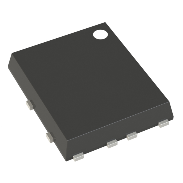
The onsemi NVMFD6H846NLT1G is a dual N-channel enhancement mode power MOSFET designed for surface mount applications. It features an 8-pin DFN package with dimensions of 5.1 mm in length and 1.05 mm in height. The device supports a maximum drain-source voltage (Vd) of 40 V and a continuous drain current (Id) of 29 A. Key electrical parameters include a maximum drain-source resistance (Rd) of 14.5 mΩ, a typical gate charge (Qg) of 6.3 nC at specified Vgs, and a forward voltage (Vf) of 0.84 V. It operates within a temperature range of -55°C to 175°C with a maximum power dissipation (Pd) of 23 W. The component is AEC-Q101 qualified.
Verify the specific suffix T1G against the official datasheet to confirm tape and reel packaging requirements. Confirm that the 40V rating aligns with system voltage headroom needs. Check for RoHS compliance status if environmental regulations apply. Ensure the DFN footprint matches the PCB layout constraints. Validate thermal management capabilities given the 23W dissipation limit.
Select this component when a dual N-channel topology is required in a small form factor. The 40V rating suits low-voltage automotive and industrial systems. Compare the 14.5mΩ Rds(on) against alternative devices for efficiency targets. Consider the 29A current capacity relative to load requirements. Evaluate the 6.3nC gate charge for driver compatibility.
This part belongs to onsemi's portfolio of automotive-grade power MOSFETs. It utilizes a DFN package to save board space compared to traditional through-hole options. The dual configuration allows for half-bridge or synchronous rectifier implementations. It is distinct from single-channel variants in the same voltage class.
Check for direct pin-compatible alternatives with similar 40V and 29A ratings. Verify that any substitute maintains the DFN 8-pin footprint and 1.05mm height. Ensure the replacement also holds AEC-Q101 certification if used in automotive contexts.
 NVMFD6H846NLT1G

The activity of extra discounts on wholesale prices is in full swing…
Please fill in your contact information and we will send you the latest wholesale price list.