ChipApex | Global Electronic Components Supplier

SEARCH
Search Product
Search Post
— IC芯片 | 连接器 | 传感器 | 被动器件 —
Search productSearch post
— IC芯片 | 连接器 | 传感器 | 被动器件 —
Consult the customer manager about the wholesale price.
consultation hotline:86-132-6715-2157
email:[email protected]
Contact the product manager for consultation. One-stop consultation is available.
Do you want a lower wholesale price? Please send us your inquiry and we will reply immediately.
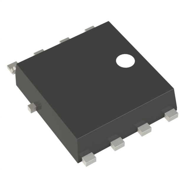
The onsemi NVMJD027N10MCLTWG is a dual N-channel power MOSFET rated for 100 V drain-to-source voltage and 28 A continuous drain current at 25°C case temperature. It features a maximum on-resistance of 26 mΩ at 10 V gate drive and 7 A drain current. The device utilizes an LFPAK8 (5x6 mm) surface-mount package with a junction-to-case thermal resistance of 3.29 °C/W. Key electrical parameters include a total gate charge of 9.9 nC at 10 V, input capacitance of 697 pF, and a single-pulse avalanche energy rating of 291 mJ. It supports a source current of 35 A and operates within a junction temperature range of -55°C to +175°C.
Verify the specific ordering suffix TWG to confirm tape and reel packaging specifications and quantity per reel. Ensure compatibility with standard reflow soldering profiles by checking lead temperature limits relative to board assembly requirements. Confirm RoHS compliance status matches project environmental standards before finalizing procurement orders.
Select this component when compact dual-channel integration is required in space-constrained designs. Evaluate thermal management needs based on the 3.29 °C/W junction-to-case resistance under steady-state conditions. Consider the 26 mΩ on-resistance for conduction loss calculations at expected operating currents and gate drive voltages.
This part belongs to onsemi's NVMJD series of dual N-channel MOSFETs designed for automotive and industrial applications. It shares the LFPAK8 footprint with other devices in the family but offers distinct electrical characteristics tailored for high-current switching. The dual configuration allows for efficient half-bridge or synchronous rectifier implementations.
Direct substitutes must match the 100 V rating, dual N-channel topology, and LFPAK8 package. Verify that alternative parts meet the same AEC-Q101 qualification and PPAP capability requirements if used in automotive contexts.
 NVMJD027N10MCLTWG

The activity of extra discounts on wholesale prices is in full swing…
Please fill in your contact information and we will send you the latest wholesale price list.