 ChipApex | Global Electronic Components Supplier

SEARCH
Search Product
Search Post
— IC芯片 | 连接器 | 传感器 | 被动器件 —
Search productSearch post
— IC芯片 | 连接器 | 传感器 | 被动器件 —
Consult the customer manager about the wholesale price.
consultation hotline:86-132-6715-2157
email:[email protected]
Contact the product manager for consultation. One-stop consultation is available.
Do you want a lower wholesale price? Please send us your inquiry and we will reply immediately.
The NX1029X is a complementary N/P-channel enhancement mode Field-Effect Transistor utilizing Trench MOSFET technology in an SOT666 package. The N-channel device supports a drain-source voltage of 60 V and continuous drain current of 330 mA, with a typical on-state resistance of 1 Ω at VGS = 10 V. The P-channel counterpart provides a drain-source voltage of -50 V and continuous drain current of -170 mA, featuring a typical on-state resistance of 4.5 Ω at VGS = -10 V. Both transistors operate within a junction temperature range of -55 °C to +150 °C.
Verify the specific ordering suffix against the manufacturer's official documentation to ensure correct packaging and marking codes. Confirm that the application environment does not require automotive qualification, as this product is explicitly designated as non-automotive qualified. Cross-reference the SOT666 footprint dimensions during PCB layout to guarantee proper surface-mount assembly compatibility.
Select this component when space-constrained designs require a complementary pair in a single ultra-small lead package. The logic-level compatibility allows direct interfacing with standard digital logic outputs without additional level shifting drivers. Evaluate thermal dissipation constraints carefully, as the small plastic package limits total power dissipation compared to larger industrial packages.
This part belongs to Nexperia's portfolio of small-signal field-effect transistors designed for high-density surface-mount applications. It utilizes advanced Trench MOSFET technology to achieve low on-resistance and fast switching speeds within the compact SOT666 outline. The complementary N/P configuration simplifies circuit design for push-pull or bridge topologies where minimal board area is critical.
NX1029XH
No, the product data sheet explicitly states that this product is not automotive qualified and is intended for general-purpose use.
The N-channel transistor (TR1) has an electrostatic discharge protection rating of up to 2 kV according to the Human Body Model (HBM).
The P-channel device exhibits a higher typical on-state resistance of 4.5 Ω at VGS = -10 V, whereas the N-channel device typically offers 1 Ω at VGS = 10 V.
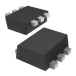 NX1029XH

The activity of extra discounts on wholesale prices is in full swing…
Please fill in your contact information and we will send you the latest wholesale price list.





