 ChipApex | Global Electronic Components Supplier

SEARCH
Search Product
Search Post
— IC芯片 | 连接器 | 传感器 | 被动器件 —
Search productSearch post
— IC芯片 | 连接器 | 传感器 | 被动器件 —
Consult the customer manager about the wholesale price.
consultation hotline:86-132-6715-2157
email:[email protected]
Contact the product manager for consultation. One-stop consultation is available.
Do you want a lower wholesale price? Please send us your inquiry and we will reply immediately.
The PHKD6N02LT is a dual N-channel TrenchMOS logic level FET in an SO8 plastic package. It features a drain-source voltage of 20 V and a continuous drain current of 10.9 A at 25 °C. The typical on-state resistance is 25 mΩ at VGS = 2.5 V. Total power dissipation is 4.17 W. Gate-drain charge is 6 nC. Junction temperature ranges from -55 to 150 °C.
Verify the specific ordering suffix against the manufacturer's official documentation to ensure correct packaging configuration. Confirm that the component meets all required environmental standards for the intended application environment before finalizing procurement decisions.
Select this component for applications requiring dual N-channel enhancement mode FETs with logic level compatibility. Ensure the design accommodates the 20 V drain-source voltage limit and the thermal constraints defined by the junction-to-solder point resistance specifications.
This device utilizes Nexperia's TrenchMOS technology within a standard SOT96-1 (SO8) plastic small outline package. It is designed specifically for computing, communications, consumer, and industrial applications as stated in the product profile.
No public confirmed substitute part numbers are available in the provided documentation.
The absolute maximum gate-source voltage is ±12 V.
No, the data sheet explicitly states it is not suitable for automotive use unless expressly stated otherwise.
The peak drain current is 44 A under pulsed conditions with a pulse width of 100 µs or less.
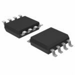 PHKD6N02LT,518

The activity of extra discounts on wholesale prices is in full swing…
Please fill in your contact information and we will send you the latest wholesale price list.





