 ChipApex | Global Electronic Components Supplier

SEARCH
Search Product
Search Post
— IC芯片 | 连接器 | 传感器 | 被动器件 —
Search productSearch post
— IC芯片 | 连接器 | 传感器 | 被动器件 —
Consult the customer manager about the wholesale price.
consultation hotline:86-132-6715-2157
email:[email protected]
Contact the product manager for consultation. One-stop consultation is available.
Do you want a lower wholesale price? Please send us your inquiry and we will reply immediately.
The PJS6816_S1_00001 is a 20V N-Channel Enhancement Mode MOSFET manufactured by Panjit International Inc. in an SOT-23 6L package. It supports a continuous drain current of 5.2A and a pulsed drain current of 20.8A. The device features low on-state resistance, with maximum values of 29mΩ at VGS=4.5V/ID=5.2A, 42mΩ at VGS=2.5V/ID=3.7A, and 85mΩ at VGS=1.8V/ID=1.6A. Key electrical parameters include a gate-source voltage limit of +12V, power dissipation of 1.25W at 25°C, and a junction temperature range of -55°C to 150°C.
Verify the specific ordering suffix against official documentation to confirm packaging details. The source material indicates that suffixes such as _S1_ correspond to 3K pcs per 7-inch reel, while _S2_ corresponds to 10K pcs per 13-inch reel. Confirming the exact suffix ensures the correct packing quantity and type are received. Always cross-reference the latest datasheet revision from the manufacturer to ensure compliance with current specifications.
Select this component for low-voltage switching applications requiring high efficiency. The low RDS(ON) across various gate drive voltages makes it suitable for systems operating at 1.8V, 2.5V, or 4.5V logic levels. Ensure the thermal design accounts for the 100°C/W junction-to-ambient thermal resistance and the 10 mW/°C derating factor above 25°C ambient temperature to maintain reliability within the specified operating range.
This part belongs to the PJS6816 series of N-Channel Enhancement Mode MOSFETs produced by Panjit International Inc. The series utilizes advanced trench process technology to achieve low on-resistance and fast switching speeds. These devices are engineered for compact surface-mount applications, offering a balance of current handling capability and thermal performance in small form-factor packages like the SOT-23 6L.
Publicly confirmed substitute part numbers are not available in the provided documentation. When evaluating alternatives, verify that any replacement matches the 20V drain-source voltage, 5.2A continuous current rating, and SOT-23 6L package dimensions. Ensure the alternative device meets the same RDS(ON) specifications at comparable gate drive voltages to maintain circuit performance.
The maximum pulsed drain current (IDM) is 20.8 A.
The typical total gate charge (Qg) is 7 nC, measured at VDS=10V, ID=5.2A, and VGS=4.5V.
No. The manufacturer explicitly states that these products are not designed or authorized for equipment requiring high reliability, life-saving instruments, or transportation equipment.
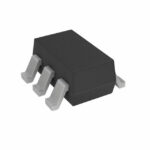 PJS6816_S1_00001

The activity of extra discounts on wholesale prices is in full swing…
Please fill in your contact information and we will send you the latest wholesale price list.





