 ChipApex | Global Electronic Components Supplier

SEARCH
Search Product
Search Post
— IC芯片 | 连接器 | 传感器 | 被动器件 —
Search productSearch post
— IC芯片 | 连接器 | 传感器 | 被动器件 —
Consult the customer manager about the wholesale price.
consultation hotline:86-132-6715-2157
email:[email protected]
Contact the product manager for consultation. One-stop consultation is available.
Do you want a lower wholesale price? Please send us your inquiry and we will reply immediately.
The PJX138K is a 50V N-Channel Enhancement Mode MOSFET in an SOT-563 package. It features advanced trench process technology and ESD protection rated at 2kV HBM. Key electrical parameters include a drain-source breakdown voltage of 50V, continuous drain current of 350mA, and pulsed drain current of 1200mA. On-state resistance is specified as less than 1.6Ω at VGS=10V/ID=500mA, less than 2.5Ω at VGS=4.5V/ID=200mA, and less than 4.5Ω at VGS=2.5V/ID=100mA. The device operates within a junction temperature range of -55°C to +150°C with a power dissipation of 223mW at 25°C ambient.
Verify the specific ordering suffix against the manufacturer's official documentation to confirm packaging quantity and reel size. The datasheet lists multiple packing options including 4K, 8K, and 10K pieces on 7-inch reels, and 20K pieces on 13-inch reels. Ensure the requested part number matches the required mechanical tape and reel specifications for automated assembly processes.
Select this component for low-voltage switching applications requiring high reliability and electrostatic discharge tolerance. The SOT-563 package provides a compact footprint suitable for space-constrained designs. Evaluate thermal performance based on the 560°C/W junction-to-ambient thermal resistance when designing heat dissipation strategies for continuous operation.
This component belongs to Panjit International Inc.'s portfolio of silicon-based enhancement mode MOSFETs. The PJX138K utilizes a single N-channel configuration designed specifically for battery-operated electronics. It represents the company's implementation of trench technology to optimize conduction losses while maintaining robustness against static discharge events common in consumer electronics manufacturing.
Publicly confirmed substitute part numbers are not available in the provided documentation. Verify pinout compatibility and electrical parameter margins before considering alternative manufacturers' components.
The maximum pulsed drain current (IDM) is 1200 mA.
The device is ESD protected up to 2KV Human Body Model (HBM).
The typical total gate charge (Qg) is 0.63 nC under test conditions of VDS=25V, ID=250mA, and VGS=4.5V.
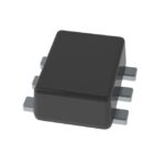 PJX138K_R1_00001

The activity of extra discounts on wholesale prices is in full swing…
Please fill in your contact information and we will send you the latest wholesale price list.





