ChipApex | Global Electronic Components Supplier

SEARCH
Search Product
Search Post
— IC芯片 | 连接器 | 传感器 | 被动器件 —
Search productSearch post
— IC芯片 | 连接器 | 传感器 | 被动器件 —
Consult the customer manager about the wholesale price.
consultation hotline:86-132-6715-2157
email:[email protected]
Contact the product manager for consultation. One-stop consultation is available.
Do you want a lower wholesale price? Please send us your inquiry and we will reply immediately.
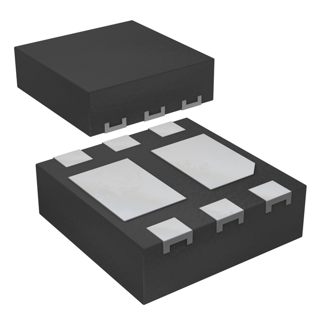
The PMDPB30XN,115 is a dual N-channel enhancement mode Field-Effect Transistor utilizing Trench MOSFET technology. It features a DFN2020-6 (SOT1118) leadless package measuring 2 x 2 x 0.65 mm with an exposed drain pad for thermal conduction. Key electrical parameters include a drain-source voltage of 20 V and a continuous drain current of 5.3 A at 25 °C. The typical on-state resistance is 32 mΩ at VGS = 4.5 V and ID = 3 A. Total gate charge is typically 14.4 nC, with turn-on delay of 4 ns and fall time of 16 ns. Operating junction temperature ranges from -55 °C to +150 °C.
Verify the specific ordering suffix
Select this component for applications requiring low profile and high thermal efficiency in small form factors. The dual channel design allows for independent control or parallel operation within a single footprint. Ensure gate drive voltages remain within the specified limits to maintain optimal RDSon performance and switching speeds.
This device belongs to Nexperia's portfolio of Trench MOSFETs, which utilize advanced silicon technology to reduce conduction losses while maintaining fast switching capabilities. The DFN2020-6 package is part of the HUSON family, offering improved thermal performance compared to traditional plastic packages of similar size.
PMDPB30XNZ is a verified substitute with identical pinout and general specifications, though it may exhibit slightly different static characteristics such as RDSon thresholds.
The maximum peak drain current is 12 A under single pulse conditions with a duration of 10 µs or less at 25 °C.
The drain-source on-state resistance increases with junction temperature; for example, it rises from a typical 32 mΩ at 25 °C to 55 mΩ at 150 °C under standard test conditions.
No, unless explicitly stated otherwise in the data sheet, this product is not suitable for automotive use and has not been qualified according to automotive testing standards.
 PMDPB30XN,115

The activity of extra discounts on wholesale prices is in full swing…
Please fill in your contact information and we will send you the latest wholesale price list.