ChipApex | Global Electronic Components Supplier

SEARCH
Search Product
Search Post
— IC芯片 | 连接器 | 传感器 | 被动器件 —
Search productSearch post
— IC芯片 | 连接器 | 传感器 | 被动器件 —
Consult the customer manager about the wholesale price.
consultation hotline:86-132-6715-2157
email:[email protected]
Contact the product manager for consultation. One-stop consultation is available.
Do you want a lower wholesale price? Please send us your inquiry and we will reply immediately.
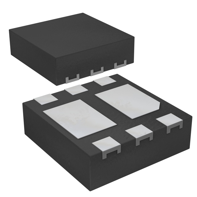
The PMDPB38UNE is a dual N-channel enhancement mode Field-Effect Transistor utilizing Trench MOSFET technology. It is housed in a leadless DFN2020-6 (SOT1118) plastic package measuring 2 x 2 x 0.65 mm with an exposed drain pad for thermal management. Key electrical parameters include a drain-source voltage of 20 V and a gate-source voltage limit of ±8 V. The device supports a continuous drain current of 5 A at 25 °C, with a typical on-state resistance of 38 mΩ at VGS = 4.5 V. Total power dissipation reaches 510 mW in free air. ESD protection is rated up to 1.6 kV via HBM.
Verify the component origin carefully, as the original NXP Standard Product business was transferred to Nexperia in February 2017. Ensure documentation references align with current manufacturer guidelines. Confirm package integrity upon receipt, as the DFN2020-6 form factor requires specific handling protocols during assembly and inspection processes.
Select this component for applications requiring low on-state resistance and high switching efficiency in space-constrained designs. The dual configuration allows for independent control or parallel operation to increase current capacity. Evaluate thermal performance based on PCB copper area, as the exposed drain pad significantly influences heat dissipation capabilities under load conditions.
This device belongs to the family of dual N-channel Trench MOSFETs designed for general-purpose power switching. It utilizes advanced trench technology to minimize resistance while maintaining robust switching characteristics. The product line targets portable electronics and computing peripherals where efficient power management and small footprint are critical design constraints.
Check for direct equivalents from Nexperia following the corporate restructuring. Verify pinout compatibility and thermal resistance values when substituting similar dual MOSFET packages. Ensure replacement parts meet the same 20 V rating and current handling requirements for the specific application circuit.
The device supports a peak drain current of 16 A under single-pulse conditions with a pulse width of 10 µs or less at 25 °C.
The drain-source on-state resistance increases with temperature; it rises from a typical 38 mΩ at 25 °C to approximately 59 mΩ at 150 °C under standard test conditions.
The thermal resistance from junction to solder point ranges from 11 K/W to 20 K/W, depending on the mounting conditions on the PCB.
 PMDPB38UNE,115

The activity of extra discounts on wholesale prices is in full swing…
Please fill in your contact information and we will send you the latest wholesale price list.