ChipApex | Global Electronic Components Supplier

SEARCH
Search Product
Search Post
— IC芯片 | 连接器 | 传感器 | 被动器件 —
Search productSearch post
— IC芯片 | 连接器 | 传感器 | 被动器件 —
Consult the customer manager about the wholesale price.
consultation hotline:86-132-6715-2157
email:[email protected]
Contact the product manager for consultation. One-stop consultation is available.
Do you want a lower wholesale price? Please send us your inquiry and we will reply immediately.
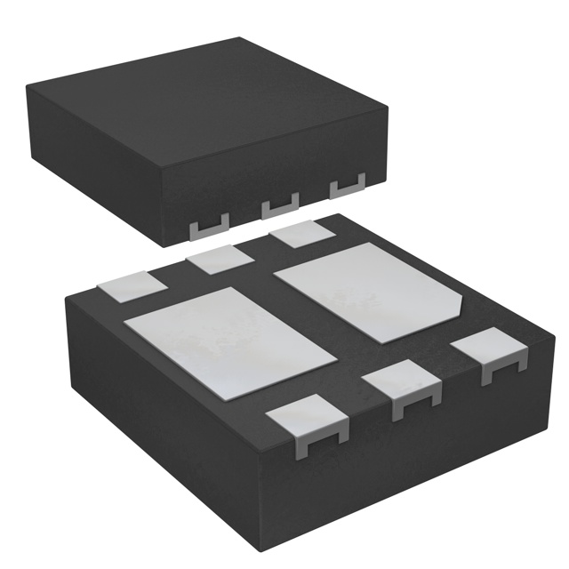
The PMDPB42UN is a dual N-channel enhancement mode Field-Effect Transistor utilizing Trench MOSFET technology. It is housed in an ultra-thin DFN2020-6 (SOT1118) leadless package measuring 2 x 2 x 0.65 mm with an exposed drain pad for thermal conduction. Key electrical parameters include a drain-source voltage of 20 V and a gate-source voltage of ±8 V. The device supports a continuous drain current of 3.9 A at 25 °C, rising to 5.1 A for short pulses. The typical on-state resistance is 40 mΩ at VGS = 4.5 V and ID = 3.9 A. Total gate charge is typically 23.5 nC.
Verify the component origin carefully as the standard product business was transferred to Nexperia. Confirm that the datasheet references align with the specific manufacturing batch requirements. Ensure the ordering suffix matches the exact package variant needed for the design. Cross-check the marking code against the official documentation to prevent counterfeit risks during assembly.
Select this component when space constraints require an ultra-thin footprint under 1 mm height. The dual configuration allows for cost-effective implementation of bridge or half-bridge topologies. Verify that the 20 V rating provides sufficient margin for the target application's supply voltage. Consider the thermal performance of the PCB layout due to the exposed pad requirement for optimal heat dissipation.
This device belongs to the family of small-signal power transistors designed for high-density electronics. It utilizes advanced trench technology to minimize on-resistance while maintaining low gate charge. The SOT1118 package is optimized for automated surface-mount assembly processes common in consumer electronics manufacturing.
Check for direct pin-compatible alternatives from the same manufacturer series. Verify that any substitute maintains the identical 20 V rating and comparable RDS(on) values. Ensure the replacement package dimensions match the existing PCB footprint to avoid mechanical interference.
 PMDPB42UN,115

The activity of extra discounts on wholesale prices is in full swing…
Please fill in your contact information and we will send you the latest wholesale price list.