ChipApex | Global Electronic Components Supplier

SEARCH
Search Product
Search Post
— IC芯片 | 连接器 | 传感器 | 被动器件 —
Search productSearch post
— IC芯片 | 连接器 | 传感器 | 被动器件 —
Consult the customer manager about the wholesale price.
consultation hotline:86-132-6715-2157
email:[email protected]
Contact the product manager for consultation. One-stop consultation is available.
Do you want a lower wholesale price? Please send us your inquiry and we will reply immediately.
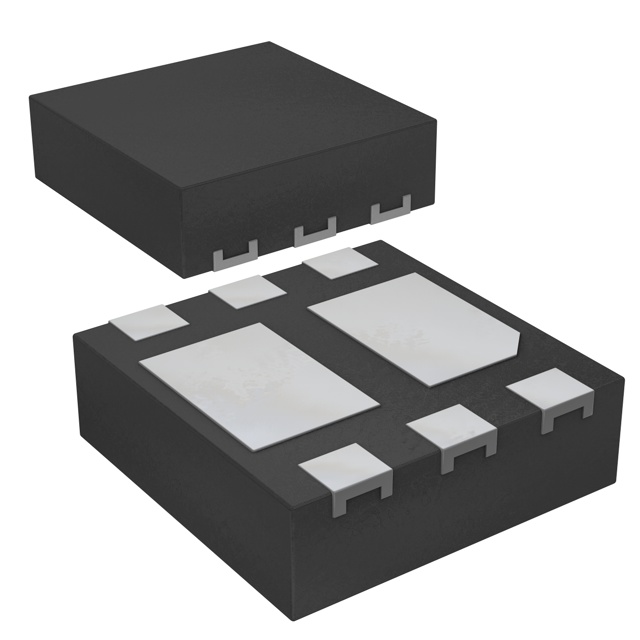
The PMDPB56XNEA is a dual N-channel enhancement mode Field-Effect Transistor utilizing Trench MOSFET technology. It features a leadless DFN2020D-6 (SOT1118D) plastic package measuring 2 x 2 x 0.65 mm. The device supports a drain-source voltage of 30 V and a continuous drain current of 3.1 A per transistor at 25 °C. Static characteristics include a maximum on-state resistance of 72 mΩ at VGS = 4.5 V. The component is qualified to the AEC-Q101 standard for automotive applications.
Verify the specific ordering suffix against official Nexperia documentation to confirm packaging configuration, as suffixes may indicate variations in reel or cut tape specifications. Ensure the procurement channel sources directly from authorized distributors to guarantee authenticity and traceability. Confirm that the delivered components match the exact part number and marking codes specified in the product data sheet.
Select this component for designs requiring compact dual N-channel switching solutions within space-constrained areas. The low threshold voltage facilitates efficient drive from low-voltage logic interfaces. Consider the thermal resistance values when designing heat dissipation strategies, particularly regarding junction-to-ambient and junction-to-solder point parameters under varying duty cycles.
This device belongs to Nexperia's portfolio of small signal and logic MOSFETs designed for surface-mount applications. It utilizes advanced Trench technology to achieve low on-resistance within an ultra-thin, leadless package. The dual configuration allows for independent control of two channels within a minimal footprint, supporting modern electronic design density requirements.
Consult official Nexperia cross-reference lists for verified substitutes. Ensure any replacement maintains identical pinout configurations, voltage ratings, and package dimensions to fit existing footprints without redesign.
The maximum non-repetitive drain-source avalanche energy is 6.2 mJ when ID is 0.3 A and the initial junction temperature is 25 °C.
The gate-source threshold voltage decreases as the junction temperature increases, ranging from a minimum of 0.75 V to a maximum of 1.25 V at 25 °C.
At VDS = 15 V and f = 1 MHz, the input capacitance is typically 256 pF, output capacitance is 31 pF, and reverse transfer capacitance is 23 pF.
 PMDPB56XNEAX

The activity of extra discounts on wholesale prices is in full swing…
Please fill in your contact information and we will send you the latest wholesale price list.