ChipApex | Global Electronic Components Supplier

SEARCH
Search Product
Search Post
— IC芯片 | 连接器 | 传感器 | 被动器件 —
Search productSearch post
— IC芯片 | 连接器 | 传感器 | 被动器件 —
Consult the customer manager about the wholesale price.
consultation hotline:86-132-6715-2157
email:[email protected]
Contact the product manager for consultation. One-stop consultation is available.
Do you want a lower wholesale price? Please send us your inquiry and we will reply immediately.
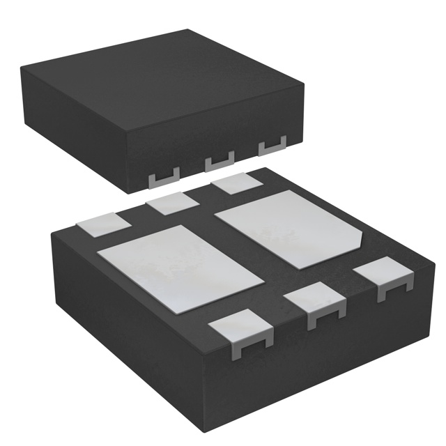
The PMDPB95XNE is a dual N-channel enhancement mode Field-Effect Transistor utilizing Trench MOSFET technology. It is housed in a leadless DFN2020-6 (SOT1118) surface-mounted package measuring 2 x 2 x 0.6 mm with an exposed drain pad for thermal conduction. Key electrical parameters include a drain-source voltage of 30 V and a continuous drain current of 2.4 A at 25 °C. The typical on-state resistance is 95 mΩ at VGS = 4.5 V and ID = 2 A. The device supports junction temperatures from -55 °C to 150 °C and offers ESD protection up to 1.8 kV.
Verify the manufacturer designation, as the product history indicates a transition from NXP Semiconductors to Nexperia B.V. Ensure the component matches the specific DFN2020-6 package outline and pin configuration defined in the official datasheet. Confirm that the sourcing channel provides authentic parts consistent with the original NXP specifications.
Select this component for applications requiring low on-state resistance and high switching efficiency in compact designs. The dual configuration allows for independent control or parallel operation within a small footprint. Consider the thermal resistance characteristics when designing heat dissipation strategies for the exposed pad.
This component belongs to the family of dual N-channel Trench MOSFETs designed for power management in portable electronics. It represents a shift towards leadless packages to improve thermal performance and reduce board space. The technology leverages trench structures to minimize resistance while maintaining robust switching capabilities.
Public confirmed substitute part numbers are not available in the provided documentation.
The device features ESD protection up to 1.8 kV, measured between all pins.
The DFN2020-6 package includes an exposed drain pad that facilitates excellent thermal conduction from the junction to the printed-circuit board.
The total gate charge is typically 1.65 nC, with a maximum of 2.5 nC under specified conditions.
 PMDPB95XNE,115

The activity of extra discounts on wholesale prices is in full swing…
Please fill in your contact information and we will send you the latest wholesale price list.