 ChipApex | Global Electronic Components Supplier

SEARCH
Search Product
Search Post
— IC芯片 | 连接器 | 传感器 | 被动器件 —
Search productSearch post
— IC芯片 | 连接器 | 传感器 | 被动器件 —
Consult the customer manager about the wholesale price.
consultation hotline:86-132-6715-2157
email:[email protected]
Contact the product manager for consultation. One-stop consultation is available.
Do you want a lower wholesale price? Please send us your inquiry and we will reply immediately.
The PMDPB95XNE2 is a dual N-channel enhancement mode Field-Effect Transistor utilizing Trench MOSFET technology. It is housed in a leadless DFN2020-6 (SOT1118) plastic package measuring 2 x 2 x 0.65 mm with an exposed drain pad for thermal conduction. The device supports a drain-source voltage of 30 V and a continuous drain current of 3 A at 25 °C. Key electrical parameters include a maximum on-state resistance of 99 mΩ at VGS = 4.5 V and ID = 2.8 A, and a gate-source threshold voltage ranging from 0.75 V to 1.25 V. Total gate charge is typically 2.9 nC, with input capacitance at 258 pF. Junction temperature ranges from -55 °C to 150 °C.
Verify the specific ordering suffix against the manufacturer's official documentation to confirm packaging configuration and reel specifications. Confirm that the component status aligns with project requirements, as availability may vary by region. Ensure design-in compliance with Nexperia's general terms and conditions regarding liability and suitability for intended applications before finalizing procurement.
Select this component for designs requiring low on-state resistance and high switching speeds in compact form factors. The dual configuration allows for efficient bridge or half-bridge topologies within limited board space. Evaluate thermal management strategies based on the junction-to-ambient thermal resistance values provided in the datasheet, particularly for high-duty cycle operations where heat dissipation through the exposed pad is critical.
This component belongs to the Nexperia PMDPB series of dual N-channel Trench MOSFETs. It shares architectural similarities with other devices in the family but is distinguished by its specific 30 V rating and DFN2020-6 package dimensions. The series targets portable electronics and power management applications requiring high efficiency and small footprint solutions.
Publicly confirmed substitute part numbers are not available in the provided source material. Verify pinout compatibility and electrical parameter margins when considering alternative manufacturers' components for direct replacement.
The maximum drain-source voltage (VDS) is rated at 30 V.
The DFN2020-6 package features an exposed drain pad that provides excellent thermal conduction from the junction to the printed-circuit board.
The typical total gate charge (QG(tot)) is 2.9 nC under standard test conditions.
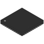 PMDPB95XNE2115

The activity of extra discounts on wholesale prices is in full swing…
Please fill in your contact information and we will send you the latest wholesale price list.





