 ChipApex | Global Electronic Components Supplier

SEARCH
Search Product
Search Post
— IC芯片 | 连接器 | 传感器 | 被动器件 —
Search productSearch post
— IC芯片 | 连接器 | 传感器 | 被动器件 —
Consult the customer manager about the wholesale price.
consultation hotline:86-132-6715-2157
email:[email protected]
Contact the product manager for consultation. One-stop consultation is available.
Do you want a lower wholesale price? Please send us your inquiry and we will reply immediately.
The PMGD8000LN is a dual N-channel enhancement mode field-effect transistor utilizing μTrenchMOS™ technology. It features a drain-source voltage (VDS) of 30 V and a continuous drain current (ID) of 125 mA at 25 °C. The device operates with a gate-source threshold voltage ranging from 0.8 V to 1.5 V. On-state resistance (RDSon) is specified as 1.8 Ω typical at VGS = 4 V and ID = 10 mA, increasing to 2.9 Ω at VGS = 2.5 V and ID = 1 mA. Total power dissipation is rated at 0.2 W at 25 °C ambient temperature. The component is housed in a SOT363 (SC-88) plastic surface mount package.
Verify the manufacturer status carefully, as the original NXP Standard Product business was rebranded as Nexperia in February 2017. Confirm that the datasheet references align with the current supplier documentation. Ensure the specific ordering code matches the required package variant and check for any updates regarding product longevity or availability status before finalizing procurement plans.
Select this component for designs requiring compact dual-switching solutions with low gate drive voltage compatibility. Evaluate the thermal resistance and power dissipation limits relative to the expected ambient operating conditions. Consider the peak drain current capabilities for pulsed applications and ensure the gate charge parameters fit the driving circuit's speed requirements.
This device belongs to the category of discrete power semiconductors designed for general-purpose switching. It represents a transition period where Philips Semiconductors products were managed under the NXP brand before the establishment of Nexperia. The part utilizes a specific trench MOS architecture optimized for low on-resistance and fast transient response in small form factors.
Consult official Nexperia documentation for verified substitute part numbers. Cross-reference pinout configurations and electrical specifications to ensure functional equivalence. Verify package dimensions and mounting requirements to confirm mechanical compatibility with existing PCB layouts.
The maximum junction temperature (Tj) is 150 °C.
The RDSon increases significantly at higher temperatures; for example, it rises from a typical 1.8 Ω at 25 °C to 2.9 Ω at 150 °C when VGS is 4 V.
The provided datasheet lists battery management and DC-to-DC converters as applications but does not explicitly state automotive qualification standards such as AEC-Q101.
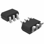 PMGD8000LN,115

The activity of extra discounts on wholesale prices is in full swing…
Please fill in your contact information and we will send you the latest wholesale price list.





