 ChipApex | Global Electronic Components Supplier
SEARCH
Search Product
Search Post
— IC芯片 | 连接器 | 传感器 | 被动器件 —
Search productSearch post
— IC芯片 | 连接器 | 传感器 | 被动器件 —
Consult the customer manager about the wholesale price.
consultation hotline:86-132-6715-2157
email:[email protected]
Contact the product manager for consultation. One-stop consultation is available.
Do you want a lower wholesale price? Please send us your inquiry and we will reply immediately.
The PMWD19UN is a dual N-channel enhancement mode field-effect transistor utilizing μTrenchMOS technology. It features a low profile plastic SOT530-1 (TSSOP8) package. The device supports a drain-source voltage of 30 V and a continuous drain current of 5.6 A at 25 °C. Total power dissipation reaches 2.3 W, with an on-state resistance of 23 mΩ maximum at VGS = 4.5 V. Gate threshold voltage ranges from 0.45 V to 0.7 V. Thermal resistance from junction to solder point is typically 55 K/W.
Verify the specific ordering suffix against the manufacturer's latest documentation to confirm package type and tape-and-reel specifications. Confirm that the component status remains active or qualified for production before initiating design-in processes. Ensure compliance with absolute maximum ratings during operation.
Select this component for applications requiring compact dual FET solutions with low drive requirements. Evaluate thermal performance based on the specified junction-to-solder point resistance. Consider the peak drain current capabilities when designing for pulsed load conditions within the safe operating area limits.
This component belongs to the μTrenchMOS family of power transistors designed for high efficiency and low conduction losses. It serves as a discrete solution for managing multiple channels in space-constrained environments where standard MOSFET footprints are prohibitive.
Consult official replacement lists for direct equivalents. Verify pinout compatibility and electrical parameters such as RDSon and VGS(th) before substituting.
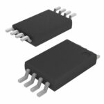 PMWD19UN,518
The activity of extra discounts on wholesale prices is in full swing…
Please fill in your contact information and we will send you the latest wholesale price list.





