 ChipApex | Global Electronic Components Supplier

SEARCH
Search Product
Search Post
— IC芯片 | 连接器 | 传感器 | 被动器件 —
Search productSearch post
— IC芯片 | 连接器 | 传感器 | 被动器件 —
Consult the customer manager about the wholesale price.
consultation hotline:86-132-6715-2157
email:[email protected]
Contact the product manager for consultation. One-stop consultation is available.
Do you want a lower wholesale price? Please send us your inquiry and we will reply immediately.
The PMWD30UN is a dual N-channel enhancement mode field-effect transistor utilizing μTrenchMOS technology. It provides two independent channels in an SOT530-1 (TSSOP8) plastic package. Key electrical parameters include a drain-source voltage of 30 V, continuous drain current up to 5 A at 25 °C, and peak drain current of 18 A. The on-state resistance is typically 30 mΩ at VGS = 4.5 V and ID = 3.5 A. Total power dissipation is rated at 2.3 W at 25 °C. Gate charge is typically 28 nC, with input capacitance of 1478 pF.
Verify the specific manufacturer origin as the datasheet references Philips Semiconductors while the brand is listed as NXP USA Inc. Confirm the package type matches the SOT530-1 outline. Check for any Customer Product/Process Change Notifications regarding design updates or availability status changes since the original publication date.
Select this component for applications requiring dual N-channel MOSFETs in a compact thin shrink small outline package. Ensure the operating junction temperature remains within the -55 °C to +150 °C range. Verify that the gate drive voltage meets the requirements for the specified on-state resistance values, particularly for low voltage logic levels.
This device belongs to the μTrenchMOS family of ultra-low level FETs designed for efficient power switching in space-constrained environments. The dual configuration allows for synchronized control or bridge topologies within a single footprint, reducing board area compared to discrete single-channel alternatives.
Consult official replacement lists for equivalent dual N-channel MOSFETs in SOT530-1 packages. Verify pinout compatibility and thermal characteristics before substitution.
The peak drain current is 18 A under pulsed conditions with a pulse width of 10 μs or less.
The on-state resistance increases with junction temperature; it rises from a typical 30 mΩ at 25 °C to 56 mΩ at 150 °C.
The reverse recovery time is typically 50 ns when sourcing 4 A with a di/dt of -100 A/μs.
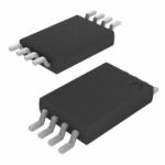 PMWD30UN,518

The activity of extra discounts on wholesale prices is in full swing…
Please fill in your contact information and we will send you the latest wholesale price list.





