ChipApex | Global Electronic Components Supplier
SEARCH
Search Product
Search Post
— IC芯片 | 连接器 | 传感器 | 被动器件 —
Search productSearch post
— IC芯片 | 连接器 | 传感器 | 被动器件 —
Consult the customer manager about the wholesale price.
consultation hotline:86-132-6715-2157
email:[email protected]
Contact the product manager for consultation. One-stop consultation is available.
Do you want a lower wholesale price? Please send us your inquiry and we will reply immediately.
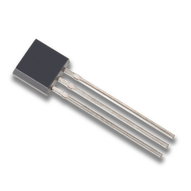
The PN4118 is an N-channel JFET amplifier in a TO-92 package. It features a gate-source breakdown voltage of -40V and a saturation drain current range of 0.08mA to 0.60mA at VDS=10V, VGS=0. The gate-source cutoff voltage spans -1V to -3V. Common-source forward transconductance ranges from 80µS to 650µS at 1kHz. Input capacitance is guaranteed up to 3pF, and reverse transfer capacitance up to 1.5pF.
Verify the specific ordering suffix matches the required package type (TO-92) and compliance status (RoHS). Confirm that the manufacturer designation aligns with Linear Integrated Systems or authorized equivalents. Ensure the component meets the specified electrical characteristics for your application requirements before finalizing procurement.
Select this component when ultra-high input impedance is critical for the design. Consider the symmetrical geometry if bidirectional signal flow is needed. Evaluate the saturation drain current and cutoff voltage ranges to ensure compatibility with the intended biasing conditions and signal levels.
This device belongs to a family of N-channel JFET amplifiers including the 2N4117A and 2N4119A variants. These components are designed for applications demanding minimal circuit loading and high input impedance. The TO-92 package provides a standard through-hole mounting option suitable for various discrete semiconductor applications.
Compatible substitutes include the 2N4118A and SST4118. Verify pinout compatibility and electrical parameter alignment, particularly regarding gate-source breakdown voltage and saturation drain current ranges, before implementing any replacement.
Yes, due to the symmetrical geometry of the device, the source and drain leads may be operated interchangeably.
The maximum gate-source or gate-drain voltage rating is -40V.
Gate reverse current increases significantly at elevated temperatures, reaching up to -2.5nA at 150°C compared to -1pA at 25°C.
 PN4118 TO-92 3L ROHS
The activity of extra discounts on wholesale prices is in full swing…
Please fill in your contact information and we will send you the latest wholesale price list.