 ChipApex | Global Electronic Components Supplier
SEARCH
Search Product
Search Post
— IC芯片 | 连接器 | 传感器 | 被动器件 —
Search productSearch post
— IC芯片 | 连接器 | 传感器 | 被动器件 —
Consult the customer manager about the wholesale price.
consultation hotline:86-132-6715-2157
email:[email protected]
Contact the product manager for consultation. One-stop consultation is available.
Do you want a lower wholesale price? Please send us your inquiry and we will reply immediately.
The PN4391 is an N-channel silicon Junction Field-Effect Transistor (JFET) manufactured by Central Semiconductor. It is housed in a TO-92-3 through-hole package and operates as a single-element device. Key electrical specifications include a gate-source breakdown voltage of 40 V, a gate-source cutoff voltage of 10 V, and a drain-source current of 150 mA at zero gate-source voltage. The component exhibits a drain-source on-resistance of 30 Ohms and a power dissipation rating of 625 mW. It supports an operating temperature range from -65°C to +150°C.
Verify the specific suffix TRE TIN/LEAD against the manufacturer's current datasheet to confirm lead composition and RoHS status, as tin/lead terminations may differ from standard RoHS-compliant variants. Confirm that the TO-92-3 package dimensions match the target PCB footprint requirements before finalizing procurement orders.
Select this component when a low-noise N-channel JFET with high input impedance is required for analog signal processing. Ensure the circuit design accommodates the 30 Ohm on-resistance and 625 mW power dissipation limits. Verify that the 40 V breakdown voltage provides sufficient margin for the intended supply voltages.
This part belongs to the PN4391 series of N-channel JFETs produced by Central Semiconductor. It is functionally similar to other industry-standard JFETs like the 2N4391, though pinouts and specific parameters should be verified against the official Central Semiconductor datasheet. The TO-92-3 package is a common plastic encapsulation for discrete transistors.
Cross-reference with Vishay's 2N4391 or SST4391 for potential functional equivalents, but verify pinout compatibility and parameter tolerances carefully. Other manufacturers' N-channel JFETs in TO-92 packages may serve as substitutes if electrical characteristics align with the application requirements.
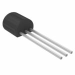 PN4391 TRE TIN/LEAD
The activity of extra discounts on wholesale prices is in full swing…
Please fill in your contact information and we will send you the latest wholesale price list.





