ChipApex | Global Electronic Components Supplier

SEARCH
Search Product
Search Post
— IC芯片 | 连接器 | 传感器 | 被动器件 —
Search productSearch post
— IC芯片 | 连接器 | 传感器 | 被动器件 —
Consult the customer manager about the wholesale price.
consultation hotline:86-132-6715-2157
email:[email protected]
Contact the product manager for consultation. One-stop consultation is available.
Do you want a lower wholesale price? Please send us your inquiry and we will reply immediately.
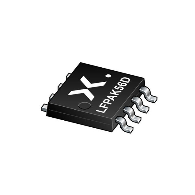
The Nexperia PSMN013-60HLX is a dual logic level N-channel MOSFET utilizing TrenchMOS technology in an LFPAK56D (SOT1205) package. It features a drain-source voltage of 60 V and a continuous drain current of 40 A at 25 °C. The typical on-state resistance is 12.5 mΩ at VGS = 5 V, reducing to 9 mΩ at VGS = 10 V. Total gate charge is 22.4 nC. The device supports a junction temperature range from -55 °C to 175 °C with a total power dissipation of 64 W.
Verify the specific ordering suffix against the manufacturer's official documentation to ensure correct packaging and tape-and-reel specifications. Confirm that the component meets RoHS compliance requirements for your target market. Cross-reference the marking code '13RL60H' with the datasheet to authenticate the physical device upon receipt.
Select this component when a compact dual-N-channel solution is required for logic-level gate drive applications. The LFPAK56D package offers a small footprint suitable for space-constrained designs. Ensure the application operates within the 60 V drain-source voltage limit and utilizes appropriate thermal management to maintain junction temperatures below 175 °C during peak load conditions.
This part belongs to the Nexperia PSMN series of silicon N-channel enhancement mode field-effect transistors. These devices are manufactured using TrenchMOS technology to achieve low on-state resistance and fast switching speeds. The series is designed for general-purpose switching applications in computing, communications, and industrial equipment sectors.
Direct substitutes include other dual N-channel MOSFETs in the SOT1205/LFPAK56D package with comparable 60 V ratings and similar RDS(on) characteristics. Verify pinout compatibility and thermal resistance values before substitution.
No, unless explicitly stated otherwise in specific product announcements, this product is not automotive qualified and is intended for computing, communications, consumer, and industrial applications.
The device is rated for 82 mJ of non-repetitive drain-source avalanche energy under specified test conditions.
At VGS = 5 V, the typical RDS(on) is 12.5 mΩ. At VGS = 10 V, the typical RDS(on) decreases to 9 mΩ.
 PSMN013-60HLX

The activity of extra discounts on wholesale prices is in full swing…
Please fill in your contact information and we will send you the latest wholesale price list.