ChipApex | Global Electronic Components Supplier

SEARCH
Search Product
Search Post
— IC芯片 | 连接器 | 传感器 | 被动器件 —
Search productSearch post
— IC芯片 | 连接器 | 传感器 | 被动器件 —
Consult the customer manager about the wholesale price.
consultation hotline:86-132-6715-2157
email:[email protected]
Contact the product manager for consultation. One-stop consultation is available.
Do you want a lower wholesale price? Please send us your inquiry and we will reply immediately.
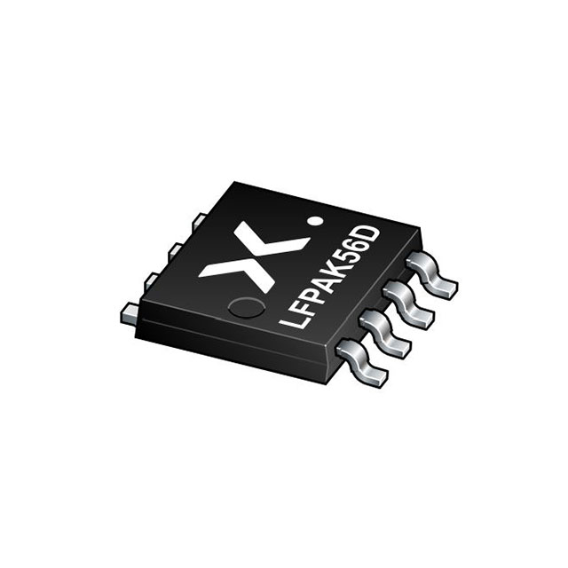
The Nexperia PSMN025-100HS is a dual standard level N-channel MOSFET utilizing TrenchMOS technology, housed in an LFPAK56D (Dual Power-SO8) package. It features a drain-source voltage of 100 V and a continuous drain current of 29.5 A at 25 °C mounting base temperature. The typical on-state resistance is 24.5 mΩ at 25 °C junction temperature, rising to 68 mΩ at 175 °C. Total power dissipation reaches 68 W under specified conditions. The device supports a maximum junction temperature of 175 °C and includes integrated source-drain diodes with a recovered charge of 62.2 nC.
Verify the specific ordering suffix against the manufacturer's official documentation to ensure correct packaging and tape-and-reel specifications. Confirm that the component meets all required environmental compliance standards for the target application. Cross-reference the marking code '25RS10H' with the datasheet to validate authenticity upon receipt. Ensure design-in compatibility with the LFPAK56D footprint dimensions provided in the package outline section.
Select this component when a dual N-channel configuration is required within a compact surface-mount footprint. The low on-state resistance and high current rating make it suitable for efficient power conversion stages. Consider the thermal resistance characteristics and the need for adequate heat sinking given the 175 °C junction temperature limit. Evaluate the gate charge requirements against the driving circuit capabilities to ensure optimal switching performance.
This device belongs to Nexperia's standard level MOSFET portfolio, leveraging TrenchMOS technology for improved efficiency. The LFPAK56D package provides a robust solution for high-power applications requiring dual channels in a single housing. It is designed for industrial and commercial equipment where reliability and thermal performance are critical. The product data sheet defines its electrical characteristics and absolute maximum ratings for design integration.
Consult the official Nexperia replacement guide or contact technical support for verified substitute part numbers. Do not assume pin-to-pin compatibility with other dual MOSFET packages without verifying electrical parameters and thermal characteristics against the original specification.
The non-repetitive drain-source avalanche energy is rated at 83 mJ under specified test conditions.
The typical on-state resistance increases from 24.5 mΩ at 25 °C to 68 mΩ at 175 °C junction temperature.
The component is housed in an LFPAK56D package, also known as Dual LFPAK or SOT1205.
 PSMN025-100HSX

The activity of extra discounts on wholesale prices is in full swing…
Please fill in your contact information and we will send you the latest wholesale price list.