ChipApex | Global Electronic Components Supplier
SEARCH
Search Product
Search Post
— IC芯片 | 连接器 | 传感器 | 被动器件 —
Search productSearch post
— IC芯片 | 连接器 | 传感器 | 被动器件 —
Consult the customer manager about the wholesale price.
consultation hotline:86-132-6715-2157
email:[email protected]
Contact the product manager for consultation. One-stop consultation is available.
Do you want a lower wholesale price? Please send us your inquiry and we will reply immediately.
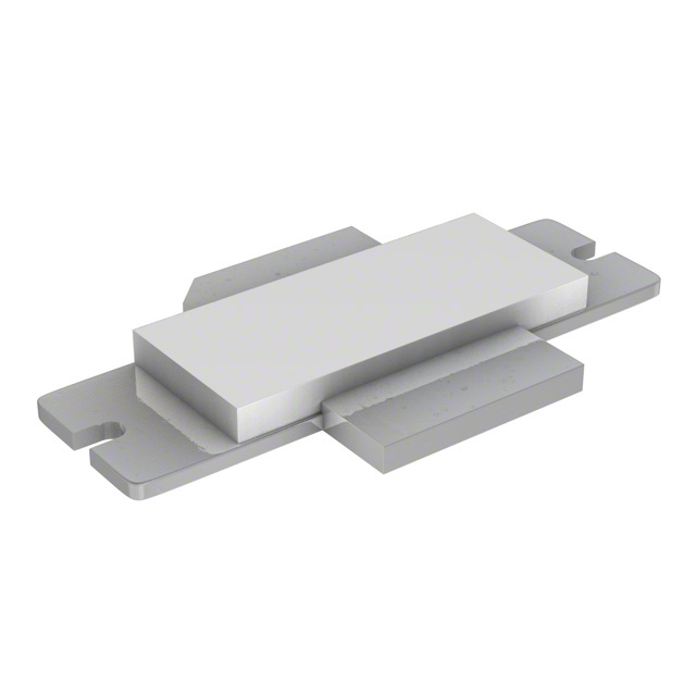
The PTFA211801E is a thermally-enhanced, 180-watt internally matched GOLDMOS FET designed for WCDMA applications. It operates from 2110 to 2170 MHz and supports single- and two-carrier configurations. Key electrical parameters include a drain-source breakdown voltage of 65 V, an on-state resistance of 0.05 Ω, and a junction temperature rating of 200 °C. The device provides a typical gain of 15.5 dB and efficiency up to 52% under CW conditions at 2170 MHz.
Verify the specific package variant required for the application. The 'E' suffix denotes Package 30260 (slotted flange), while 'F' denotes Package 31260 (earless flange). Confirm that the thermal interface and mounting hardware align with the selected package outline specifications before finalizing procurement.
Select this component for high-power RF applications requiring robust thermal performance in the 2110–2170 MHz range. Ensure the biasing network accommodates the specified operating gate voltage and quiescent current. Verify that the system can handle the maximum total device dissipation and junction temperature limits during peak operation.
This part belongs to Infineon's GOLDMOS family of LDMOS transistors. It is characterized specifically for 3GPP WCDMA signals. The datasheet includes reference circuit schematics and impedance data for integration into standard RF amplifier designs using Rogers TMM4 substrates.
The PTFA211801F is the direct alternative differing only in package type (31260 vs 30260). No other cross-model replacements are documented in the provided source material.
The maximum junction temperature (TJ) is rated at 200 °C.
Yes, the PTFA211801E features broadband internal matching.
The drain-source breakdown voltage (V(BR)DSS) is 65 V.
 PTFA211801E V4
The activity of extra discounts on wholesale prices is in full swing…
Please fill in your contact information and we will send you the latest wholesale price list.