ChipApex | Global Electronic Components Supplier
SEARCH
Search Product
Search Post
— IC芯片 | 连接器 | 传感器 | 被动器件 —
Search productSearch post
— IC芯片 | 连接器 | 传感器 | 被动器件 —
Consult the customer manager about the wholesale price.
consultation hotline:86-132-6715-2157
email:[email protected]
Contact the product manager for consultation. One-stop consultation is available.
Do you want a lower wholesale price? Please send us your inquiry and we will reply immediately.
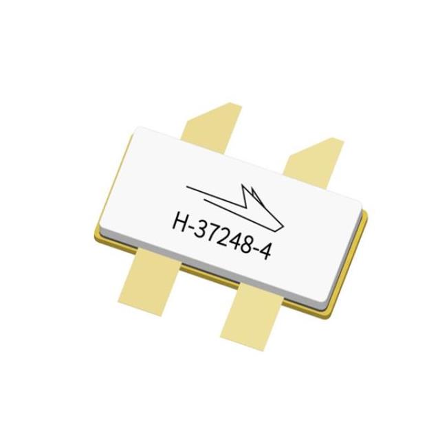
The PTFC210202FC is a dual N-channel RF power MOSFET designed for high-efficiency linear amplifier applications. It operates with a drain-source voltage of 65 V and features an internal gate bias circuit that simplifies drive requirements. The device utilizes Infineon’s advanced GaN-on-SiC technology to achieve low on-resistance and high breakdown voltage. Packaged in the H-37248-4 form factor, it provides robust thermal performance suitable for demanding wireless infrastructure environments.
Verify the exact ordering suffix against official documentation to ensure correct package and tape/reel specifications. Confirm RoHS compliance status and material content declarations prior to integration. Cross-reference datasheet revision numbers to validate electrical characteristics and mechanical dimensions match current production standards.
Select this component for designs requiring high linearity and efficiency in broadband RF applications. Evaluate thermal management strategies based on the specific PCB layout and cooling methods available. Ensure the driving circuitry aligns with the internal gate bias requirements to maximize performance and stability under varying load conditions.
This part belongs to Infineon's portfolio of GaN-based RF power transistors. These devices are engineered to replace traditional LDMOS technologies in certain frequency bands, offering superior power density and switching capabilities. The product line targets modern telecommunications standards requiring compact and efficient signal amplification solutions.
Consult official cross-reference guides for verified substitutes. Verify pinout compatibility and thermal resistance parameters before considering alternative components.
It utilizes Gallium Nitride on Silicon Carbide (GaN-on-SiC) technology.
No, it features an internal gate bias circuit that simplifies the drive requirements.
The maximum drain-source voltage is rated at 65 V.
 PTFC210202FCV1XWSA1
The activity of extra discounts on wholesale prices is in full swing…
Please fill in your contact information and we will send you the latest wholesale price list.