ChipApex | Global Electronic Components Supplier
SEARCH
Search Product
Search Post
— IC芯片 | 连接器 | 传感器 | 被动器件 —
Search productSearch post
— IC芯片 | 连接器 | 传感器 | 被动器件 —
Consult the customer manager about the wholesale price.
consultation hotline:86-132-6715-2157
email:[email protected]
Contact the product manager for consultation. One-stop consultation is available.
Do you want a lower wholesale price? Please send us your inquiry and we will reply immediately.
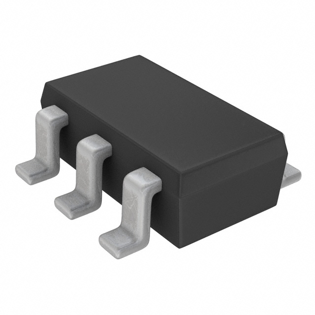
The QS6J11TR is a dual P-channel MOSFET designed for low-voltage drive applications, specifically operating with a gate-source voltage of -1.5V. It features a TSMT6 (SOT-457T) surface-mount package and is RoHS compliant. The device supports a drain-source voltage of -12V and a continuous drain current of -2A. At the typical -1.5V drive, the on-resistance is 0.2Ω, reducing to 0.075Ω at -4.5V. Total gate charge is 6.5nC, with power dissipation rated at 1.25W. Operating temperatures range from -55°C to 150°C.
Verify that the QS6J11TR is not recommended for new designs. Confirm availability through existing customer support channels rather than standard ordering systems. Ensure the specific TSMT6 package and taping format match the required assembly specifications before proceeding with any acquisition steps.
Select this component only if maintaining compatibility with existing designs requiring a dual P-channel MOSFET driven at 1.5V. Evaluate the -12V rating and 0.2Ω on-resistance against circuit requirements. Consider that newer alternatives may be available if the design is not constrained by legacy hardware requirements.
The QS6J11TR belongs to ROHM's series of small-signal MOSFETs intended for low-voltage drive scenarios. It utilizes the SOT-457T JEITA package code. The product status indicates it is produced solely to support existing customers and is discontinued for new design implementations.
No direct replacement part numbers are documented in the provided source material. Designers should consult official manufacturer resources for potential successor components or alternative packages suitable for similar low-voltage dual P-channel applications.
 QS6J11TR
The activity of extra discounts on wholesale prices is in full swing…
Please fill in your contact information and we will send you the latest wholesale price list.