ChipApex | Global Electronic Components Supplier
SEARCH
Search Product
Search Post
— IC芯片 | 连接器 | 传感器 | 被动器件 —
Search productSearch post
— IC芯片 | 连接器 | 传感器 | 被动器件 —
Consult the customer manager about the wholesale price.
consultation hotline:86-132-6715-2157
email:[email protected]
Contact the product manager for consultation. One-stop consultation is available.
Do you want a lower wholesale price? Please send us your inquiry and we will reply immediately.
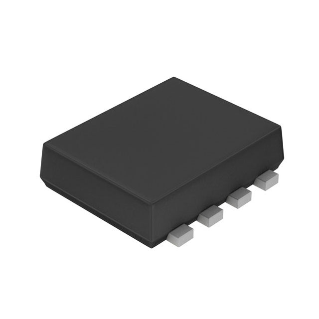
The QS8M12TCR is a dual MOSFET component manufactured by ROHM Semiconductor, integrating one N-channel and one P-channel silicon transistor within a TSMT-8 surface-mount package. The device supports low-voltage drive applications with a specified gate-source voltage of ±20 V. Key electrical parameters include a drain-source breakdown voltage of ±30 V and a continuous drain current rating of ±4 A. The typical static drain-source on-state resistance is 45 mΩ for the N-channel at VGS=4V and 60 mΩ for the P-channel at VGS=-4V. Total gate charge values are 3.4 nC for the N-channel and 8.4 nC for the P-channel. Power dissipation is rated at 1.5 W total, with an operating temperature range from -55°C to +150°C.
Verify the specific ordering suffix TCR against official documentation to confirm taping specifications and basic ordering unit quantities. Ensure that the selected variant matches the required packaging format for automated assembly processes. Cross-reference the manufacturer's latest datasheet revision to confirm all absolute maximum ratings and electrical characteristics prior to final procurement decisions.
Select this component based on the requirement for a complementary N-channel and P-channel pair in a single compact package. Evaluate the 45 mΩ and 60 mΩ on-state resistances against the target load current requirements. Confirm compatibility with the 4V drive voltage level and ensure the thermal management strategy accommodates the 1.5 W total power dissipation limit within the specified ambient temperature range.
The QS8M12 belongs to the QS8 series of 4V drive complementary MOSFETs produced by ROHM Semiconductor. This series is designed to provide integrated switching solutions for low-voltage applications. The TSMT-8 package offers a small footprint suitable for space-constrained designs while maintaining adequate thermal performance for general-purpose switching tasks.
The QH8MA2 is documented as a similar level replacement part with the same pinout and package configuration. Verify electrical parameter alignment before substitution.
The typical RDS(on) for the N-channel is 45 mΩ when measured at a drain current of 4A and a gate-source voltage of 4V.
Yes, the component includes body diodes for both the N-channel and P-channel transistors, as indicated by the inner circuit diagram and source-drain characteristics.
Operation in the maximum safe operating area is limited by the RDS(on) characteristic, particularly under DC and long pulse width conditions.
 QS8M12TCR
The activity of extra discounts on wholesale prices is in full swing…
Please fill in your contact information and we will send you the latest wholesale price list.