ChipApex | Global Electronic Components Supplier
SEARCH
Search Product
Search Post
— IC芯片 | 连接器 | 传感器 | 被动器件 —
Search productSearch post
— IC芯片 | 连接器 | 传感器 | 被动器件 —
Consult the customer manager about the wholesale price.
consultation hotline:86-132-6715-2157
email:[email protected]
Contact the product manager for consultation. One-stop consultation is available.
Do you want a lower wholesale price? Please send us your inquiry and we will reply immediately.
The SAV-551+ is an ultra-low noise, medium current E-PHEMT transistor manufactured by Mini-Circuits. It operates within a frequency range of 0.045 to 6 GHz and requires external biasing and matching circuits. The device utilizes enhancement mode Pseudomorphic High Electron Mobility Transistor technology, allowing operation with a single positive supply voltage. Key electrical specifications include a typical gain of 16 dB at 2 GHz, a maximum output IP3 of +25 dBm, and a power output at 1 dB compression of +18 dBm. It draws a low current of 15 mA and features a plastic molded SOT-343 (SC-70) package.
Verify the specific RoHS compliance status through official manufacturer documentation before integration. Confirm that the MMM1362 case style matches your PCB footprint requirements. Ensure external biasing components are selected to maintain the specified drain-source voltage and drain current limits. Check for any updated environmental or export classification data directly from the supplier.
Select this component when designing amplifiers requiring high linearity and minimal signal degradation in the RF front end. The device is ideal for applications where low noise figure is critical below 2.5 GHz. Designers must provide their own input and output matching networks as the unit is a bare die transistor. Consider the TAMP family if integrated modules with built-in matching are preferred over discrete design.
The SAV-551+ belongs to the SAV series of E-PHEMT transistors produced by Mini-Circuits. These devices are engineered for high-performance RF applications requiring low power consumption and high stability. The product line supports various wireless communication standards and is available in surface-mount packages for automated assembly processes.
The datasheet identifies the Avago ATF-55143 as a potential replacement model. Suitability for substitution depends entirely on system-specific electrical criteria, stimulus conditions, and environmental stresses. Customers must verify compatibility with existing circuit designs before implementing this change.
Yes, external biasing and matching circuits are required. The device does not include internal DC blocking or stabilization components.
The maximum operating temperature is +85 °C, while the minimum operating temperature is -40 °C.
Pin 3 serves as the Gate terminal and is used for the RF input signal.
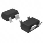 SAV-551+
The activity of extra discounts on wholesale prices is in full swing…
Please fill in your contact information and we will send you the latest wholesale price list.