ChipApex | Global Electronic Components Supplier
SEARCH
Search Product
Search Post
— IC芯片 | 连接器 | 传感器 | 被动器件 —
Search productSearch post
— IC芯片 | 连接器 | 传感器 | 被动器件 —
Consult the customer manager about the wholesale price.
consultation hotline:86-132-6715-2157
email:[email protected]
Contact the product manager for consultation. One-stop consultation is available.
Do you want a lower wholesale price? Please send us your inquiry and we will reply immediately.
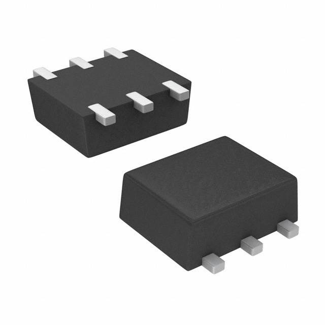
The Vishay Siliconix SI1035X-T1-E3 is a complementary N- and P-channel MOSFET in an SC-89 package. It features TrenchFET technology with a 20 V drain-source voltage rating. The N-channel exhibits a maximum on-resistance of 5 Ω at VGS = 4.5 V, while the P-channel shows 8 Ω at VGS = -4.5 V. Continuous drain current reaches 190 mA for the N-channel and -155 mA for the P-channel at 25 °C. The device supports 1.5 V operation, has a typical gate threshold voltage of ±0.9 V, and offers a 2000 V gate-source ESD rating.
Verify component authenticity through authorized distributors or direct manufacturer channels. Confirm RoHS compliance status and check for Halogen-free certification per IEC 61249-2-21 standards. Validate that the ordering suffix matches the lead-free specification. Ensure storage conditions adhere to recommended temperature ranges to maintain device reliability prior to assembly.
Select this component for applications demanding minimal footprint and low-voltage compatibility. Evaluate thermal performance against the specified junction-to-ambient resistance when designing for continuous operation. Consider the specific on-resistance values at target gate voltages to ensure adequate current handling. Verify that the required switching speed aligns with the typical turn-on and turn-off time parameters provided in the datasheet.
This part belongs to the Vishay Siliconix Si1035X series, which provides complementary MOSFET solutions. The standard ordering designation is Si1035X-T1-GE3, indicating the lead-free and halogen-free variant. The device utilizes the SC-89 (SOT-563F) package, offering a compact form factor suitable for space-constrained portable electronics and mobile communication devices.
Publicly confirmed substitute part numbers are not available in the verified documentation.
The absolute maximum gate-source voltage rating is ±5 V.
Yes, the datasheet specifies that the device is designed for 1.5 V operation.
The typical total gate charge (Qg) for the N-channel is 750 pC under test conditions of VDS = 10 V, VGS = 4.5 V, and ID = 150 mA.
 SI1035X-T1-E3
The activity of extra discounts on wholesale prices is in full swing…
Please fill in your contact information and we will send you the latest wholesale price list.