 ChipApex | Global Electronic Components Supplier
SEARCH
Search Product
Search Post
— IC芯片 | 连接器 | 传感器 | 被动器件 —
Search productSearch post
— IC芯片 | 连接器 | 传感器 | 被动器件 —
Consult the customer manager about the wholesale price.
consultation hotline:86-132-6715-2157
email:[email protected]
Contact the product manager for consultation. One-stop consultation is available.
Do you want a lower wholesale price? Please send us your inquiry and we will reply immediately.
The SI4532DY is a dual N- and P-channel enhancement mode field effect transistor manufactured by onsemi using high cell density DMOS technology. It operates with a drain-source voltage of 30 V for the N-channel and -30 V for the P-channel. The continuous drain current ratings are 3.9 A for the N-channel and -3.5 A for the P-channel. Static drain-source on-resistance is specified at 0.065 Ohms (N-channel) and 0.085 Ohms (P-channel) at VGS = 10 V. Total gate charge is typically 15 nC. The device is housed in an SOIC-8 package and supports an operating junction temperature range from -55°C to +150°C.
Verify the specific ordering suffix against official documentation to confirm packaging details such as tape and reel specifications. Ensure compliance with RoHS directives and lead-free requirements when sourcing components for production. Cross-reference datasheet revision numbers to validate electrical characteristics against current manufacturing standards.
Select this component for designs requiring complementary N- and P-channel MOSFETs in a compact footprint. Evaluate thermal resistance values based on the specific copper pad area used on the printed circuit board. Confirm that the required switching speeds and on-state resistance meet the efficiency targets of the target application.
This part belongs to the family of dual MOSFETs produced by onsemi utilizing proprietary DMOS technology. It is designed to minimize on-state resistance while providing high power handling capability in widely used surface mount packages suitable for portable electronics.
Consult official substitution guides or manufacturer databases for verified equivalent parts. Verify pinout compatibility, voltage ratings, and thermal characteristics before implementing any alternative components in existing designs.
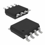 SI4532DY
The activity of extra discounts on wholesale prices is in full swing…
Please fill in your contact information and we will send you the latest wholesale price list.





