ChipApex | Global Electronic Components Supplier
SEARCH
Search Product
Search Post
— IC芯片 | 连接器 | 传感器 | 被动器件 —
Search productSearch post
— IC芯片 | 连接器 | 传感器 | 被动器件 —
Consult the customer manager about the wholesale price.
consultation hotline:86-132-6715-2157
email:[email protected]
Contact the product manager for consultation. One-stop consultation is available.
Do you want a lower wholesale price? Please send us your inquiry and we will reply immediately.
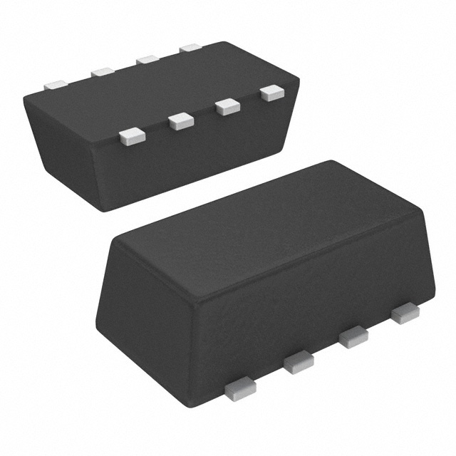
The SI5513DC-T1-GE3 is a complementary N/P-channel MOSFET array housed in a 1206-8 ChipFET package. It features a drain-source voltage of 20 V. The N-channel device supports a continuous drain current of 3.1 A, while the P-channel device supports 2.1 A. Maximum power dissipation is rated at 1.1 W. The component utilizes TrenchFET technology for low on-resistance and fast switching characteristics.
Verify the specific ordering suffix when sourcing replacements. The E3 suffix indicates lead-free composition, whereas the GE3 suffix denotes both lead-free and halogen-free compliance. Confirm that the required environmental certification matches the project specifications before procurement to ensure regulatory adherence.
Select this component for designs requiring a matched N/P pair in minimal space. The 20 V rating suits low-voltage systems. Evaluate thermal constraints as the 1.1 W dissipation limit is modest. Ensure gate drive voltages remain within the specified limits to maintain reliable operation without exceeding maximum ratings.
This part belongs to the Siliconix ChipFET family, which integrates discrete MOSFETs into standard passive footprints. The SI5513DC variant specifically provides complementary functionality, allowing designers to replace separate components with a single dual-device solution, thereby reducing board area and assembly complexity.
 SI5513DC-T1-GE3
The activity of extra discounts on wholesale prices is in full swing…
Please fill in your contact information and we will send you the latest wholesale price list.