ChipApex | Global Electronic Components Supplier
SEARCH
Search Product
Search Post
— IC芯片 | 连接器 | 传感器 | 被动器件 —
Search productSearch post
— IC芯片 | 连接器 | 传感器 | 被动器件 —
Consult the customer manager about the wholesale price.
consultation hotline:86-132-6715-2157
email:[email protected]
Contact the product manager for consultation. One-stop consultation is available.
Do you want a lower wholesale price? Please send us your inquiry and we will reply immediately.
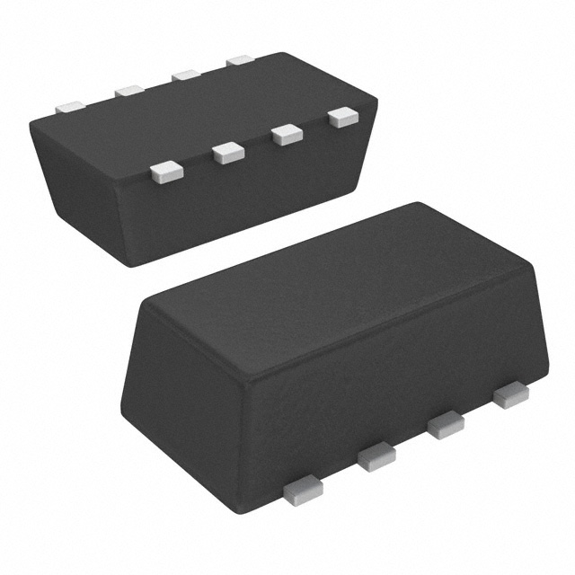
The Vishay Siliconix SI5515CDC-T1-E3 is a dual-channel MOSFET featuring complementary N- and P-Channel configurations in a leadless 1206-8 ChipFET package. It utilizes TrenchFET technology with a 20 V drain-source voltage rating. The N-Channel exhibits an on-resistance of 0.036 Ω at VGS = 4.5 V, while the P-Channel shows 0.100 Ω at VGS = -4.5 V. Continuous drain current reaches 4 A for both channels at TC = 25 °C. Total gate charge is typically 6.5 nC for the N-Channel and 6.2 nC for the P-Channel.
Verify component authenticity by checking the marking code EH against lot traceability records. Confirm RoHS compliance status via official documentation. Ensure soldering procedures account for the exposed copper terminals characteristic of the leadless 1206-8 package singulation process.
Select this component when board space constraints require a footprint comparable to standard passive components but necessitating power semiconductor performance. Evaluate thermal resistance requirements based on specific PCB copper spreading patterns, as junction-to-ambient resistance varies significantly with pad design.
This device belongs to the 1206-8 ChipFET family, designed to replace larger packages like SO-8 while maintaining equivalent thermal dissipation capabilities. It integrates two independent power switches into a compact form factor suitable for high-density surface mount applications.
SI5515CDC-T1-GE3 (Lead-free and Halogen-free variant)
 SI5515CDC-T1-E3
The activity of extra discounts on wholesale prices is in full swing…
Please fill in your contact information and we will send you the latest wholesale price list.