ChipApex | Global Electronic Components Supplier
SEARCH
Search Product
Search Post
— IC芯片 | 连接器 | 传感器 | 被动器件 —
Search productSearch post
— IC芯片 | 连接器 | 传感器 | 被动器件 —
Consult the customer manager about the wholesale price.
consultation hotline:86-132-6715-2157
email:[email protected]
Contact the product manager for consultation. One-stop consultation is available.
Do you want a lower wholesale price? Please send us your inquiry and we will reply immediately.
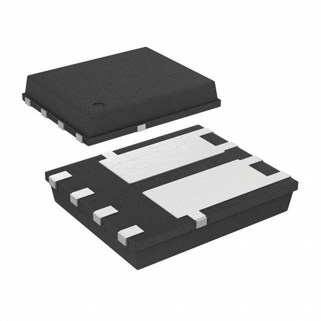
The Si7252DP-T1-GE3 is a dual N-channel 100 V (D-S) MOSFET manufactured by Vishay Siliconix. It utilizes TrenchFET power technology and is housed in a PowerPAK SO-8 Dual package. The device features a maximum drain-source voltage of 100 V and a continuous drain current of 36.7 A at TC = 25 °C. On-state resistance is specified as 0.018 Ω max at VGS = 10 V, 0.019 Ω max at VGS = 7.5 V, and 0.021 Ω max at VGS = 6 V. Typical gate charge is 12.2 nC at VDS = 50 V, VGS = 6 V, and ID = 10 A. Maximum power dissipation is 46 W at TC = 25 °C. Operating junction and storage temperature range spans from -55 to +150 °C.
Verify the specific ordering suffix against official documentation to confirm lead-free status and packaging type. Confirm that the component meets RoHS and REACH requirements for the target market. Ensure the supplier provides traceability data consistent with Vishay manufacturing protocols. Validate datasheet revision numbers before finalizing procurement specifications.
Select this component when a dual N-channel MOSFET with 100 V breakdown voltage is required in a compact surface-mount footprint. Evaluate thermal performance based on the application's ambient temperature and available copper area for heat dissipation. Consider the low on-resistance characteristics for efficiency in high-current synchronous rectification or inverter applications.
This part belongs to the Vishay Siliconix PowerPAK SO-8 Dual series. It shares the standard SO-8 footprint while accommodating a larger die size similar to DPAK packages. This design allows for direct substitution in existing layouts while providing superior thermal performance compared to traditional leaded packages.
Direct pin-compatible replacements within the same family include SI7252DV-T1-GE3. Verify electrical parameters and thermal characteristics carefully when substituting across different manufacturers or package types.
The maximum junction-to-case (drain) thermal resistance is 2.7 °C/W under steady-state conditions.
Yes, the datasheet specifies single pulse avalanche current (IAS) of 20 A and single pulse avalanche energy (EAS) of 20 mJ.
The typical body diode reverse recovery time (trr) is 39 ns at IF = 10 A, dI/dt = 100 A/μs, and TJ = 25 °C.
 SI7252DP-T1-GE3
The activity of extra discounts on wholesale prices is in full swing…
Please fill in your contact information and we will send you the latest wholesale price list.