ChipApex | Global Electronic Components Supplier
SEARCH
Search Product
Search Post
— IC芯片 | 连接器 | 传感器 | 被动器件 —
Search productSearch post
— IC芯片 | 连接器 | 传感器 | 被动器件 —
Consult the customer manager about the wholesale price.
consultation hotline:86-132-6715-2157
email:[email protected]
Contact the product manager for consultation. One-stop consultation is available.
Do you want a lower wholesale price? Please send us your inquiry and we will reply immediately.
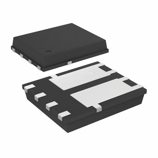
The Si7272DP-T1-GE3 is a dual N-channel MOSFET from Vishay Siliconix, utilizing TrenchFET technology. It features a 30 V drain-source voltage rating and a maximum continuous drain current of 25 A at a case temperature of 25 °C. The device exhibits a typical on-state resistance of 9.3 mΩ at VGS = 10 V and 12.4 mΩ at VGS = 4.5 V. Total gate charge is typically 8.2 nC at VGS = 4.5 V. It operates within a junction temperature range of -55 °C to +150 °C and is housed in a leadless PowerPAK SO-8 Dual package.
Verify the component against official Vishay datasheet specifications before integration. Confirm that the PowerPAK SO-8 Dual land pattern matches the recommended layout guidelines to ensure proper thermal performance and solder joint reliability during assembly.
Select this component for designs requiring two isolated N-channel switches in a compact footprint. Evaluate the thermal resistance characteristics relative to the PCB copper area, as the package relies heavily on board-level heat spreading for optimal junction-to-ambient performance under steady-state conditions.
This part belongs to the Si7272 series of dual MOSFETs manufactured by Vishay Siliconix. It shares the PowerPAK SO-8 Dual form factor with other devices in the family but is distinguished by its specific 30 V breakdown voltage and low on-resistance characteristics tailored for high-efficiency power management.
Direct pin-compatible replacements within the same package require matching dual N-channel topology and similar electrical ratings. Verify thermal resistance and gate charge parameters when substituting to maintain circuit stability and switching speed.
The maximum operating junction temperature is +150 °C.
The maximum on-resistance is 9.3 mΩ at VGS = 10 V and increases to 12.4 mΩ at VGS = 4.5 V.
Yes, the pin arrangement and dimensions match standard SO-8 devices, allowing direct substitution on existing layouts.
 SI7272DP-T1-GE3
The activity of extra discounts on wholesale prices is in full swing…
Please fill in your contact information and we will send you the latest wholesale price list.