ChipApex | Global Electronic Components Supplier
SEARCH
Search Product
Search Post
— IC芯片 | 连接器 | 传感器 | 被动器件 —
Search productSearch post
— IC芯片 | 连接器 | 传感器 | 被动器件 —
Consult the customer manager about the wholesale price.
consultation hotline:86-132-6715-2157
email:[email protected]
Contact the product manager for consultation. One-stop consultation is available.
Do you want a lower wholesale price? Please send us your inquiry and we will reply immediately.
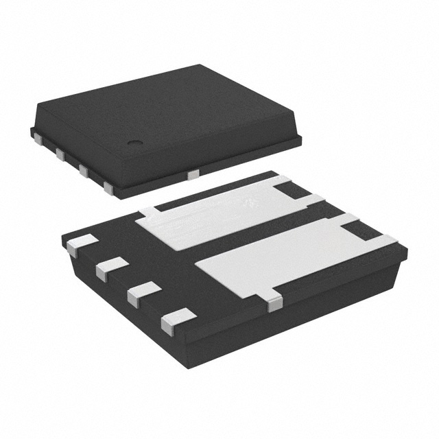
The Vishay Siliconix SI7540DP-T1-E3 is a dual N- and P-channel MOSFET in a PowerPAK SO-8 package. It features a 12 V drain-source voltage rating with an on-state resistance of 0.017 Ω for the N-channel and 0.032 Ω for the P-channel at VGS = 4.5 V. Continuous drain currents reach 11.8 A (N-channel) and -8.9 A (P-channel). The device utilizes TrenchFET technology, operates within a junction temperature range of -55 °C to 150 °C, and includes halogen-free construction.
Verify component authenticity by checking manufacturer markings against official datasheet specifications. Confirm RoHS compliance status and ensure the lead-free designation matches the specific ordering suffix requirements for your manufacturing process.
Evaluate thermal management requirements based on the specified junction-to-ambient resistance values. Ensure gate drive voltages align with the threshold characteristics for optimal switching performance. Verify that the continuous current ratings meet the peak load demands of the target application circuit.
This component belongs to the Vishay Siliconix Si7540 series of low-voltage dual MOSFETs. It is designed as a complementary pair to facilitate compact power stage designs in space-constrained environments where efficient heat dissipation is critical.
The Si7540DP-T1-GE3 is a verified alternative offering identical electrical characteristics with explicit halogen-free certification according to IEC 61249-2-21 standards.
The maximum operating junction temperature is 150 °C.
Yes, the device meets solder reflow reliability requirements with a recommended peak temperature of 260 °C.
The typical total gate charge for the N-channel is 11.5 nC under standard test conditions.
 SI7540DP-T1-E3
The activity of extra discounts on wholesale prices is in full swing…
Please fill in your contact information and we will send you the latest wholesale price list.