ChipApex | Global Electronic Components Supplier
SEARCH
Search Product
Search Post
— IC芯片 | 连接器 | 传感器 | 被动器件 —
Search productSearch post
— IC芯片 | 连接器 | 传感器 | 被动器件 —
Consult the customer manager about the wholesale price.
consultation hotline:86-132-6715-2157
email:[email protected]
Contact the product manager for consultation. One-stop consultation is available.
Do you want a lower wholesale price? Please send us your inquiry and we will reply immediately.
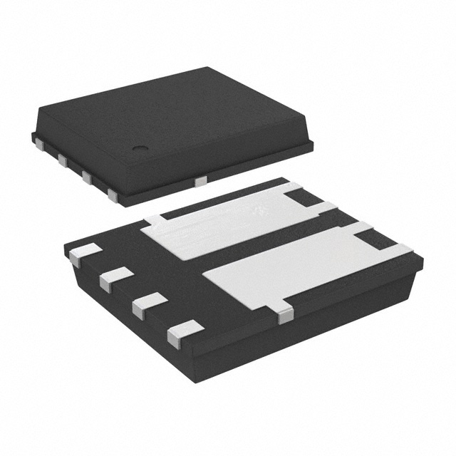
The Vishay Siliconix SI7540DP-T1-GE3 is a dual N- and P-channel MOSFET utilizing TrenchFET technology in a leadless PowerPAK SO-8 package. It features a 12 V drain-source voltage rating with an on-state resistance of 17 mΩ for the N-channel at VGS = 4.5 V and 32 mΩ for the P-channel at VGS = -4.5 V. The device supports continuous drain currents of 11.8 A (N-channel) and -8.9 A (P-channel). Designed for high-efficiency PWM applications, it includes optimized gate charge characteristics suitable for 500 kHz operation.
Verify component authenticity through authorized distributors or direct manufacturer channels. Confirm RoHS compliance and halogen-free status against current datasheet revisions. Validate package markings and lot codes to ensure alignment with the specified PowerPAK SO-8 form factor before integration into production assemblies.
Select this component for designs requiring compact dual-channel solutions with low thermal resistance. Ensure gate drive voltages align with the specified thresholds for optimal RDS(on) performance. Evaluate thermal management requirements based on the junction-to-ambient resistance values provided in the datasheet specifications.
This part belongs to the Vishay Siliconix Si7540DP series, representing a specific variant within their TrenchFET Power MOSFET lineup. It utilizes the PowerPAK SO-8 package, which offers a footprint compatible with standard SO-8 layouts while providing superior thermal dissipation capabilities due to its exposed drain pad design.
Direct pin-compatible replacements within the same package family include the Si7540DP-GE3. Verify that substitute components maintain identical voltage ratings, current capacities, and thermal characteristics to ensure circuit compatibility without layout modifications.
The operating junction and storage temperature range extends from -55 °C to +150 °C.
The PowerPAK SO-8 provides a direct, low-resistance thermal path via an exposed copper drain pad, significantly reducing junction-to-ambient thermal resistance compared to traditional leaded packages.
Yes, the device is PWM optimized with gate charge parameters specifically tuned for efficient operation at frequencies up to 500 kHz.
 SI7540DP-T1-GE3
The activity of extra discounts on wholesale prices is in full swing…
Please fill in your contact information and we will send you the latest wholesale price list.