ChipApex | Global Electronic Components Supplier
SEARCH
Search Product
Search Post
— IC芯片 | 连接器 | 传感器 | 被动器件 —
Search productSearch post
— IC芯片 | 连接器 | 传感器 | 被动器件 —
Consult the customer manager about the wholesale price.
consultation hotline:86-132-6715-2157
email:[email protected]
Contact the product manager for consultation. One-stop consultation is available.
Do you want a lower wholesale price? Please send us your inquiry and we will reply immediately.
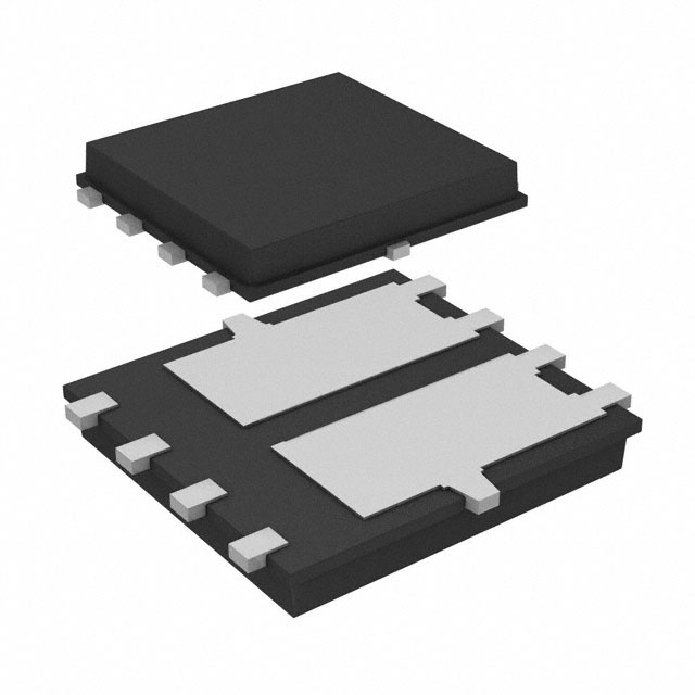
The Vishay Siliconix SI7900AEDN-T1-E3 is a dual N-channel MOSFET with a common drain configuration, housed in a PowerPAK 1212-8 package. It features a 20 V drain-source voltage rating and an 8.5 A continuous drain current capacity at 25 °C. The device exhibits low on-state resistance, with maximum values of 0.026 Ω at VGS = 4.5 V, 0.030 Ω at VGS = 2.5 V, and 0.036 Ω at VGS = 1.8 V. Key electrical parameters include a typical total gate charge (Qg) of 10.5 nC and a forward transconductance of 25 S. The component provides 3000 V ESD protection and operates within a junction temperature range of -55 °C to +150 °C.
Verify the specific ordering suffix when sourcing components. The -E3 suffix indicates lead-free construction, while the -GE3 suffix denotes both lead-free and halogen-free compliance. Confirm that the received parts match the required material categorization standards for your assembly process. Always validate datasheet specifications against the manufacturer's latest documentation prior to finalizing procurement orders.
Select this component for designs requiring dual N-channel MOSFETs in a minimal footprint. The low RDS(on) across various gate voltages makes it suitable for battery-powered systems where efficiency is critical. Ensure the PCB layout accommodates the PowerPAK 1212-8 dimensions and utilizes adequate copper spreading to maximize thermal dissipation capabilities.
This part belongs to the Vishay Siliconix Si7900 series of dual N-channel MOSFETs. It shares the PowerPAK 1212-8 package form factor with other Vishay devices designed for high-density surface-mount applications. The common drain configuration distinguishes it from standard single or half-bridge arrangements found in similar packages.
Direct substitutes must match the 20 V rating, dual N-channel common drain configuration, and PowerPAK 1212-8 package. Verify pinout compatibility and thermal resistance characteristics before implementation.
The absolute maximum rating for gate-source voltage (VGS) is ±12 V.
RDS(on) increases as gate voltage decreases: 0.026 Ω max at 4.5 V, 0.030 Ω max at 2.5 V, and 0.036 Ω max at 1.8 V.
Yes, the operating junction temperature range extends up to +150 °C.
 SI7900AEDN-T1-E3
The activity of extra discounts on wholesale prices is in full swing…
Please fill in your contact information and we will send you the latest wholesale price list.