ChipApex | Global Electronic Components Supplier
SEARCH
Search Product
Search Post
— IC芯片 | 连接器 | 传感器 | 被动器件 —
Search productSearch post
— IC芯片 | 连接器 | 传感器 | 被动器件 —
Consult the customer manager about the wholesale price.
consultation hotline:86-132-6715-2157
email:[email protected]
Contact the product manager for consultation. One-stop consultation is available.
Do you want a lower wholesale price? Please send us your inquiry and we will reply immediately.
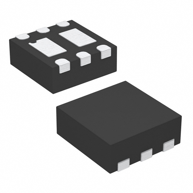
The SiA777EDJ-T1-GE3 is a dual MOSFET from Vishay Siliconix, integrating one N-channel and one P-channel device in a single PowerPAK SC-70-6 package. The N-channel component features a drain-source voltage of 20 V and an on-resistance of 0.225 Ω at VGS = 4.5 V. The P-channel counterpart provides a drain-source voltage of -12 V with an on-resistance of 0.057 Ω at VGS = -4.5 V. Both channels operate within a junction temperature range of -55 °C to +150 °C.
Verify the specific ordering suffix T1-GE3 to confirm lead-free and halogen-free compliance. Confirm that the PowerPAK SC-70-6 package dimensions match the target PCB footprint. Ensure the design accounts for the exposed copper terminals characteristic of this leadless package singulation process.
Select this component when space-constrained designs require both high-side and low-side switching capabilities in a minimal footprint. The integrated nature simplifies layout compared to discrete components. Verify that the gate drive voltages align with the specified RDS(on) thresholds for optimal efficiency.
This part belongs to the SiA777EDJ series, which pairs complementary N- and P-channel MOSFETs. It utilizes Vishay's TrenchFET technology to achieve low on-resistance within the compact PowerPAK SC-70-6 surface-mount package designed for automated assembly.
Direct replacements must maintain the dual N/P-channel configuration and PowerPAK SC-70-6 footprint. Verify that substitute parts meet or exceed the 20 V / -12 V breakdown ratings and thermal resistance specifications.
The N-channel typically offers ESD protection up to 2800 V.
The PowerPAK SC-70 is a leadless package where the terminal ends are exposed copper; manual soldering with an iron is not recommended.
Yes, the SiA777EDJ-T1-GE3 is compliant with the RoHS Directive 2002/95/EC and is halogen-free.
 SIA777EDJ-T1-GE3
The activity of extra discounts on wholesale prices is in full swing…
Please fill in your contact information and we will send you the latest wholesale price list.