 ChipApex | Global Electronic Components Supplier
SEARCH
Search Product
Search Post
— IC芯片 | 连接器 | 传感器 | 被动器件 —
Search productSearch post
— IC芯片 | 连接器 | 传感器 | 被动器件 —
Consult the customer manager about the wholesale price.
consultation hotline:86-132-6715-2157
email:[email protected]
Contact the product manager for consultation. One-stop consultation is available.
Do you want a lower wholesale price? Please send us your inquiry and we will reply immediately.
The InterFET SMP4117 is an N-Channel JFET in a SOT23 surface-mount package. It features a gate-to-source breakdown voltage of -40V and a typical gate leakage current of 1pA at VGS=-20V. The device exhibits a gate-to-source cutoff voltage range of -0.6V to -1.8V and a drain-to-source saturation current between 0.03mA and 0.09mA. Forward transconductance ranges from 70μS to 210μS, with input capacitance typically at 3pF. Continuous power dissipation is rated at 350mW, supporting junction temperatures up to 150°C.
Verify the specific suffix against official documentation to confirm packaging type and binning options. Confirm RoHS compliance status and lead material specifications prior to integration. Ensure thermal derating requirements are met for the target operating environment. Validate that the selected variant matches the required electrical parameters for the design.
Select this component for applications requiring ultra-high input impedance and femtoampere-level signal handling. Consider the SOT23 package for space-constrained surface-mount designs. Evaluate the trade-off between low leakage and required transconductance levels. Verify compatibility with existing PCB land patterns and soldering profiles.
The SMP4117 belongs to the 2N4117/A series of N-Channel JFETs manufactured by InterFET. It utilizes InterFET's N0001H geometry to achieve superior radiation hardness compared to standard silicon devices. The part serves as a surface-mount alternative to through-hole variants like the PN4117 or 2N4117.
Officially documented industry standard cross-references include SST4117, MMBF4117, and VCR7N. Verify pinout compatibility and electrical parameter limits before substitution.
Yes, the datasheet notes that source and drain pins are interchangeable.
The typical gate leakage current is 120fA at 20V, with a maximum specified limit of 1pA at room temperature.
Yes, the parts are RoHS, REACH, and CMR compliant.
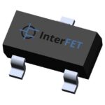 SMP4117
The activity of extra discounts on wholesale prices is in full swing…
Please fill in your contact information and we will send you the latest wholesale price list.





