ChipApex | Global Electronic Components Supplier
SEARCH
Search Product
Search Post
— IC芯片 | 连接器 | 传感器 | 被动器件 —
Search productSearch post
— IC芯片 | 连接器 | 传感器 | 被动器件 —
Consult the customer manager about the wholesale price.
consultation hotline:86-132-6715-2157
email:[email protected]
Contact the product manager for consultation. One-stop consultation is available.
Do you want a lower wholesale price? Please send us your inquiry and we will reply immediately.
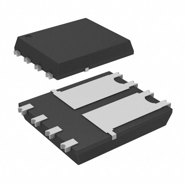
The SQS966ENW-T1_GE3 is an automotive-grade dual N-channel MOSFET from Vishay Siliconix, utilizing TrenchFET technology. It features a 60 V drain-source voltage rating and operates up to a junction temperature of 175 °C. The device is housed in a compact PowerPAK 1212-8W package with a thermal resistance (junction-to-case) of 5.4 °C/W. At VGS = 10 V, the on-state resistance is typically 0.028 Ω (max 0.036 Ω), supporting a continuous drain current of 6 A. It meets AEC-Q101 standards and undergoes 100% Rg and UIS testing.
Verify component authenticity by cross-referencing the marking code Q027 against official Vishay documentation. Confirm that the specific suffix -T1 indicates the reel packaging format. Ensure compliance with RoHS directives as specified in the product summary. Validate that the supplier provides traceability to authorized manufacturing locations.
Select this component when a dual N-channel topology is required in a minimal footprint. The 60 V rating suits standard automotive electrical systems. Evaluate the 0.036 Ω maximum on-resistance against thermal dissipation limits at 27.8 W. Consider the 5.4 °C/W junction-to-case resistance for PCB copper plane design to ensure adequate heat spreading.
This part belongs to the SQS series of automotive MOSFETs manufactured by Vishay Siliconix. It shares the PowerPAK 1212-8W form factor with other devices in the lineup but is distinguished by its dual-channel layout and 60 V breakdown voltage. The series emphasizes high thermal performance relative to its physical dimensions.
SQS966ENW-T1_GE3
The maximum pulsed drain current (IDM) is rated at 24 A under pulse test conditions with a width of 300 μs and duty cycle of 2%.
Yes, the datasheet confirms that 100% of units are tested for unclamped inductive switching (UIS). The single pulse avalanche energy (EAS) is rated at 7.2 mJ.
The on-resistance increases with junction temperature. At TC = 125 °C, the maximum RDS(on) rises to 0.055 Ω, and at TC = 175 °C, it reaches 0.066 Ω when VGS = 10 V.
 SQS966ENW-T1_GE3
The activity of extra discounts on wholesale prices is in full swing…
Please fill in your contact information and we will send you the latest wholesale price list.