ChipApex | Global Electronic Components Supplier
SEARCH
Search Product
Search Post
— IC芯片 | 连接器 | 传感器 | 被动器件 —
Search productSearch post
— IC芯片 | 连接器 | 传感器 | 被动器件 —
Consult the customer manager about the wholesale price.
consultation hotline:86-132-6715-2157
email:[email protected]
Contact the product manager for consultation. One-stop consultation is available.
Do you want a lower wholesale price? Please send us your inquiry and we will reply immediately.
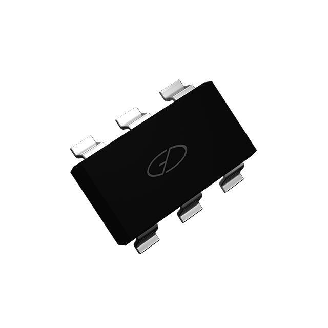
The SSFK2219 is a dual P-channel MOSFET in an SOT-363 package. It features a drain-source voltage of -20V and a continuous drain current of -540mA at 25°C. The on-resistance is typically 440mΩ at VGS=-4.5V, rising to 850mΩ at -2.5V. Gate charge is typically 1nC. Thermal resistance junction-to-ambient is 450°C/W. Operating temperature ranges from -55°C to +150°C.
Verify the specific datasheet revision (Doc.USSSFK2219xSP3.1) matches your design requirements. Confirm that the SOT-363 package dimensions align with your PCB footprint. Ensure thermal management strategies account for the specified junction-to-ambient resistance under your expected operating conditions.
Select this component for low-voltage, low-current dual P-channel applications requiring minimal board space. The low gate charge supports efficient operation in high-frequency switching environments. Verify that the -20V rating exceeds your maximum circuit voltage and that the -540mA current capacity meets load requirements.
This device belongs to Good-Ark Semiconductor's MOSFET portfolio, utilizing advanced processing techniques to achieve high cell density. The dual configuration integrates two independent P-channel devices into a single SOT-363 package, reducing component count compared to discrete solutions.
No public confirmed substitute part numbers are available in the provided documentation.
The maximum pulsed drain current (IDM) is -2.16 A.
RDS(ON) is typically 440mΩ at VGS=-4.5V, 850mΩ at VGS=-2.5V, and 1200mΩ at VGS=-1.8V.
The storage temperature range is -55°C to +150°C.
 SSFK2219
The activity of extra discounts on wholesale prices is in full swing…
Please fill in your contact information and we will send you the latest wholesale price list.