ChipApex | Global Electronic Components Supplier
SEARCH
Search Product
Search Post
— IC芯片 | 连接器 | 传感器 | 被动器件 —
Search productSearch post
— IC芯片 | 连接器 | 传感器 | 被动器件 —
Consult the customer manager about the wholesale price.
consultation hotline:86-132-6715-2157
email:[email protected]
Contact the product manager for consultation. One-stop consultation is available.
Do you want a lower wholesale price? Please send us your inquiry and we will reply immediately.
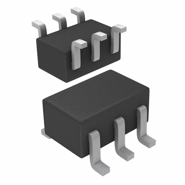
The SSM6L09FU is a dual-channel silicon MOSFET from Toshiba, integrating one N-channel and one P-channel enhancement-mode transistor within a compact UF-6 package. The N-channel device (Q1) supports a drain-source voltage of 30 V with a maximum on-resistance of 0.7 Ω at VGS = 10 V. The P-channel device (Q2) provides a drain-source voltage of -30 V and a maximum on-resistance of 2.7 Ω at VGS = -10 V. Both channels operate within a junction temperature range up to 150 °C and share a total power dissipation rating of 300 mW.
Verify the specific ordering suffix against official Toshiba documentation to confirm exact packaging configurations. Ensure that the selected variant matches the required tape-and-reel specifications for automated assembly processes. Cross-reference the manufacturer part number with authorized distributor catalogs to validate component authenticity and traceability before finalizing procurement orders.
Select this component when a compact dual-transistor solution is required for low-voltage power switching. The N-channel unit suits positive rail control, while the P-channel unit handles negative or high-side switching tasks. Evaluate thermal derating requirements carefully, as the total power dissipation is limited to 300 mW on standard FR4 substrates.
This component belongs to Toshiba's discrete field-effect transistor lineup designed for consumer and industrial electronics. It utilizes the UF-6 package to minimize footprint while maintaining reliable electrical isolation between the two internal channels. The product represents a cost-effective alternative to using separate discrete N-channel and P-channel MOSFETs in dual-switching topologies.
Direct replacements must match the UF-6 package dimensions and provide comparable RDS(ON) values at equivalent gate voltages. Verify that substitute components maintain similar threshold voltage ranges and capacitance profiles to ensure circuit stability without redesigning the driving logic.
 SSM6L09FUTE85LF
The activity of extra discounts on wholesale prices is in full swing…
Please fill in your contact information and we will send you the latest wholesale price list.