ChipApex | Global Electronic Components Supplier
SEARCH
Search Product
Search Post
— IC芯片 | 连接器 | 传感器 | 被动器件 —
Search productSearch post
— IC芯片 | 连接器 | 传感器 | 被动器件 —
Consult the customer manager about the wholesale price.
consultation hotline:86-132-6715-2157
email:[email protected]
Contact the product manager for consultation. One-stop consultation is available.
Do you want a lower wholesale price? Please send us your inquiry and we will reply immediately.
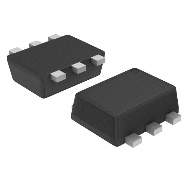
The SSM6L14FE(TE85L,F) is a dual-channel silicon MOSFET featuring one N-channel and one P-channel transistor in an ES-6 (SOT-563) package. The N-channel device supports a drain-source voltage of 20 V, with a maximum on-resistance of 240 mΩ at VGS = 4.5 V and 330 mΩ at VGS = 2.5 V. The P-channel device operates at -20 V, offering a maximum on-resistance of 300 mΩ at VGS = -4.5 V and 440 mΩ at VGS = -2.5 V. Both channels are designed for 1.5-V drive applications. Absolute maximum ratings include a DC drain current of 0.8 A for the N-channel and -0.72 A for the P-channel, with a total power dissipation of 150 mW.
Verify the specific ordering suffix TE85L,F to confirm tape-and-reel packaging quantities. Ensure compatibility with RoHS directives if required by the target market regulations. Confirm that the ES-6 footprint matches the PCB layout design before finalizing component selection.
Select this component when a complementary N/P pair is needed for low-voltage logic interfaces or load switching. Evaluate thermal derating curves based on the FR4 board copper pad area, as power dissipation is limited to 150 mW. Verify that the gate drive voltage meets the minimum threshold requirements for the desired on-resistance performance.
This part belongs to Toshiba's U-MOSIII series of small-signal MOSFETs. It is manufactured using silicon technology and is designed for surface-mount assembly. The device is intended for portable electronics and battery-powered systems where space constraints and low standby currents are critical design factors.
Direct substitutes must match the ES-6 package, 20V rating, and dual N/P configuration. Verify pinout compatibility and electrical parameters such as RDS(on) and Vth against the original datasheet specifications.
 SSM6L14FE(TE85L,F)
The activity of extra discounts on wholesale prices is in full swing…
Please fill in your contact information and we will send you the latest wholesale price list.