ChipApex | Global Electronic Components Supplier
SEARCH
Search Product
Search Post
— IC芯片 | 连接器 | 传感器 | 被动器件 —
Search productSearch post
— IC芯片 | 连接器 | 传感器 | 被动器件 —
Consult the customer manager about the wholesale price.
consultation hotline:86-132-6715-2157
email:[email protected]
Contact the product manager for consultation. One-stop consultation is available.
Do you want a lower wholesale price? Please send us your inquiry and we will reply immediately.
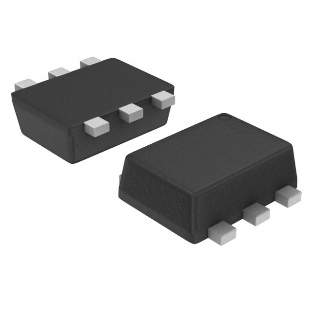
The SSM6L56FE,LM is a dual-channel silicon MOSFET containing one N-channel and one P-channel enhancement-mode transistor in an ES6 package. It supports high-speed switching with a 1.5-V drive capability. The N-channel Q1 offers a maximum drain-source on-resistance of 235 mΩ at VGS = 4.5 V and ID = 800 mA. The P-channel Q2 provides a maximum RDS(ON) of 390 mΩ at VGS = -4.5 V and ID = -800 mA. Both channels share a ±8 V gate-source voltage rating and support a continuous drain current of ±800 mA. Power dissipation is rated at 150 mW, with an operating temperature range from -55°C to +150°C.
Verify the specific ordering code suffix against official Toshiba documentation to confirm packaging and tape specifications. Ensure that the component source matches the manufacturer's authorized distribution channels to guarantee authenticity and traceability. Confirm RoHS compliance status directly with the supplier prior to procurement.
Select this component when a complementary N/P-channel pair is required in a minimal footprint. Evaluate the on-resistance requirements against the available gate drive voltage, as RDS(ON) increases significantly below 2.5 V. Verify thermal management capabilities, as the 150 mW power dissipation limit requires adequate PCB copper area for heat spreading.
This device belongs to Toshiba's small-signal MOSFET portfolio designed for portable electronics and battery-powered systems. It utilizes advanced cell technology to achieve low resistance within the ES6 package. The dual configuration allows for efficient half-bridge or push-pull driver implementations without requiring separate components.
SSM6L14FE(TE85L,F)
 SSM6L56FE,LM
The activity of extra discounts on wholesale prices is in full swing…
Please fill in your contact information and we will send you the latest wholesale price list.