ChipApex | Global Electronic Components Supplier
SEARCH
Search Product
Search Post
— IC芯片 | 连接器 | 传感器 | 被动器件 —
Search productSearch post
— IC芯片 | 连接器 | 传感器 | 被动器件 —
Consult the customer manager about the wholesale price.
consultation hotline:86-132-6715-2157
email:[email protected]
Contact the product manager for consultation. One-stop consultation is available.
Do you want a lower wholesale price? Please send us your inquiry and we will reply immediately.
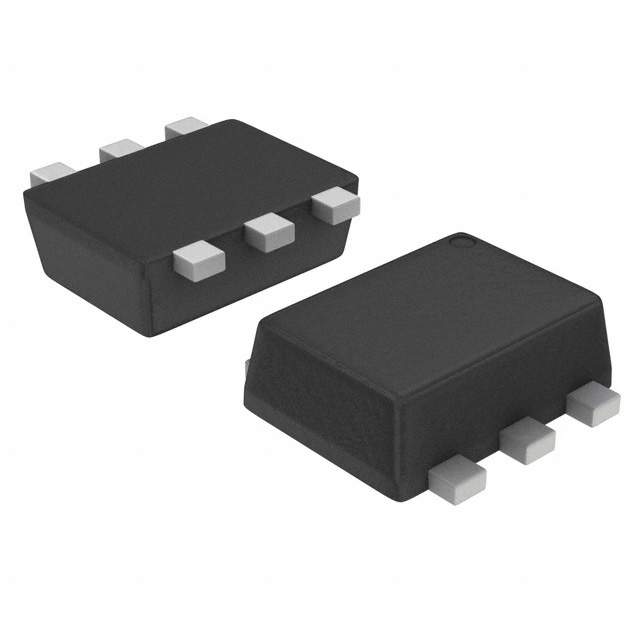
The Toshiba SSM6N44FE,LM is a dual N-channel silicon MOSFET in an ES6-6 surface-mount package. It features a drain-source breakdown voltage of 30 V and a continuous drain current of 100 mA. The device has a maximum on-resistance of 4.0 Ω at VGS = 4 V and 7.0 Ω at VGS = 2.5 V. Gate-source voltage limits are ±20 V, with a threshold voltage up to 1.5 V. Power dissipation is rated at 150 mW, operating between -55°C and +150°C. Switching times include a turn-on time of 50 ns and turn-off time of 200 ns.
Verify the specific ordering suffix against official documentation to confirm packaging details such as reel or cut tape specifications. Ensure compliance with AEC-Q101 automotive qualification requirements if applicable to the target design. Confirm RoHS status and environmental declarations prior to final procurement decisions.
Select this component when a dual N-channel MOSFET with low on-resistance is required in a small footprint. Consider the 30 V drain-source voltage rating and 100 mA current limit for appropriate load matching. Evaluate thermal derating curves for operation above 25°C ambient temperature to ensure reliability within the 150 mW power dissipation limit.
This part belongs to the SSM6N44 series of dual N-channel MOSFETs manufactured by Toshiba Semiconductor and Storage. It utilizes the MOSVI trademark technology. The component is designed for general-purpose switching tasks requiring compact integration and reliable performance in consumer and industrial electronics.
Check for direct equivalents within the same series or package family. Verify pinout compatibility and electrical parameter alignment before substitution.
The absolute maximum gate-source voltage (VGSS) is rated at ±20 V.
The maximum on-resistance is 4.0 Ω at VGS = 4 V and increases to 7.0 Ω at VGS = 2.5 V.
The typical turn-on time is 50 ns and the typical turn-off time is 200 ns under standard test conditions.
 SSM6N44FE,LM
The activity of extra discounts on wholesale prices is in full swing…
Please fill in your contact information and we will send you the latest wholesale price list.