ChipApex | Global Electronic Components Supplier
SEARCH
Search Product
Search Post
— IC芯片 | 连接器 | 传感器 | 被动器件 —
Search productSearch post
— IC芯片 | 连接器 | 传感器 | 被动器件 —
Consult the customer manager about the wholesale price.
consultation hotline:86-132-6715-2157
email:[email protected]
Contact the product manager for consultation. One-stop consultation is available.
Do you want a lower wholesale price? Please send us your inquiry and we will reply immediately.
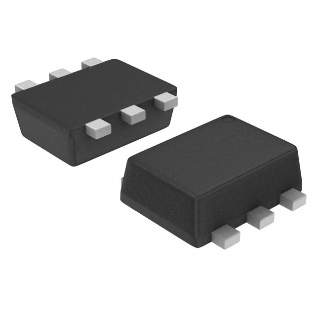
The SSM6N7002BFE is a dual N-channel silicon MOSFET from Toshiba, utilizing U-MOS IV technology. It features a compact ES6 package with a drain-source voltage (VDSS) of 60 V and a continuous DC drain current (ID) of 200 mA. The device offers low on-resistance, specified as 3.3 Ω max at VGS = 4.5 V, 2.6 Ω max at VGS = 5 V, and 2.1 Ω max at VGS = 10 V. Gate-source voltage (VGSS) is rated at ±20 V, with a gate threshold voltage (Vth) ranging from 1.5 V to 3.1 V. Power dissipation (PD) is 150 mW, operating within a temperature range of -55°C to +150°C.
Verify the specific ordering suffix against the manufacturer's official documentation to confirm exact packaging and tape specifications. Ensure compliance with RoHS directives and environmental regulations relevant to your region before procurement. Confirm that the supplier provides valid traceability documents for quality assurance purposes.
Select this component when a dual N-channel MOSFET with low on-resistance is required in a minimal footprint. Consider the 150 mW power dissipation limit and ensure adequate thermal management on the PCB. Verify that the gate drive voltage aligns with the desired RDS(ON) performance characteristics for optimal efficiency.
This part belongs to Toshiba's U-MOS IV series, designed for general-purpose switching. It serves as a compact solution for replacing discrete single transistors in dual-channel configurations. The ES6 package facilitates automated surface-mount assembly, supporting high-volume manufacturing requirements for consumer and industrial electronics.
Direct substitutes include the SSM6N7002KFU,LF and SSM6N7002BFU,LT, which share similar electrical ratings and package types. Verify pinout compatibility and thermal characteristics before substitution. Cross-reference datasheets to ensure equivalent switching speeds and breakdown voltages match the original design requirements.
 SSM6N7002BFE,LM
The activity of extra discounts on wholesale prices is in full swing…
Please fill in your contact information and we will send you the latest wholesale price list.