ChipApex | Global Electronic Components Supplier
SEARCH
Search Product
Search Post
— IC芯片 | 连接器 | 传感器 | 被动器件 —
Search productSearch post
— IC芯片 | 连接器 | 传感器 | 被动器件 —
Consult the customer manager about the wholesale price.
consultation hotline:86-132-6715-2157
email:[email protected]
Contact the product manager for consultation. One-stop consultation is available.
Do you want a lower wholesale price? Please send us your inquiry and we will reply immediately.
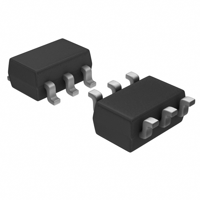
The SSM6N7002KFU,LF is a dual N-channel small-signal MOSFET manufactured by Toshiba Semiconductor and Storage. It utilizes U-MOSVII-H technology within a compact SOT-363-6 surface-mount package. Key electrical parameters include a drain-source breakdown voltage (Vds) of 60 V and a continuous drain current (Id) of 300 mA. The device features a maximum on-resistance (Rds(on)) of 1.5 Ohms at a gate-source voltage of 10 V. It operates with a gate-source voltage range of ±20 V and has a typical gate charge (Qg) of 390 pC. Thermal performance includes a power dissipation (Pd) of 500 mW and an operating temperature range from -55°C to +150°C.
Verify the specific ordering suffix against official Toshiba documentation to ensure correct packaging and RoHS compliance status. Confirm that the SOT-363-6 footprint matches the target PCB layout requirements. Check for any automotive qualification markings if the application requires AEC-Q101 certification, as standard commercial versions may differ from qualified variants.
Select this component when a dual N-channel configuration is required in a minimal footprint. Ensure the 60 V voltage rating and 300 mA current capacity exceed the circuit's maximum operational demands. Consider the 1.5 Ohm on-resistance for power loss calculations in low-voltage applications. Verify thermal management capabilities given the 500 mW power dissipation limit in the SOT-363-6 package.
This part belongs to the SSM6N7002 series of dual N-channel MOSFETs. It shares similar electrical characteristics with other members like SSM6N7002KFU,LXH but differs in packaging and specific pinout configurations. The series is designed for general-purpose switching and signal handling in consumer electronics.
Direct substitutes are not explicitly confirmed in public datasheets. Evaluate alternatives based on matching Vds, Id, Rds(on), and package dimensions. Verify pin compatibility before replacement to avoid circuit redesign.
 SSM6N7002KFU,LF
The activity of extra discounts on wholesale prices is in full swing…
Please fill in your contact information and we will send you the latest wholesale price list.